150W Multiple Output DC UPS System

Abstract

A Direct Current Uninterruptible Power Supply system is a special version of UPS providing a regulated DC output to power typical low/medium-power DC devices.

The DC UPS described in this article is using a lithium battery pack as backup energy storage and is powered by a 150W 24V DC switching power supply. It provides regulated DC outputs for 5V, 12V and 19V devices.

The backup battery pack is composed by five lithium iron phosphate (LiFePo4) batteries connected in series providing a nominal voltage of 16V (3.2V x 5). The battery model adopted in this project has 32700 form factor (32mm diameter x 70mm height) rated for 7ah capacity. As a consequence, the global power capacity (see ref. [1]) of the battery pack is 112Wh. This is about 15% than a traditional AC UPS in the same range of output power equipped with a typical 12v/7ah lead acid battery corresponding to 96Wh. Furthermore, the power density of lithium batteries is increasing over the time and you can easily find same form factor batteries rated for 12800mah that in the same configuration would be able to provide the outstanding power of 204Wh!

Here follows a picture (front view) of the assembled UPS. The front side of the case hosts an OLED display, a knob driving a rotary encoder/button, the connector to update the firmware and the battery fuse.
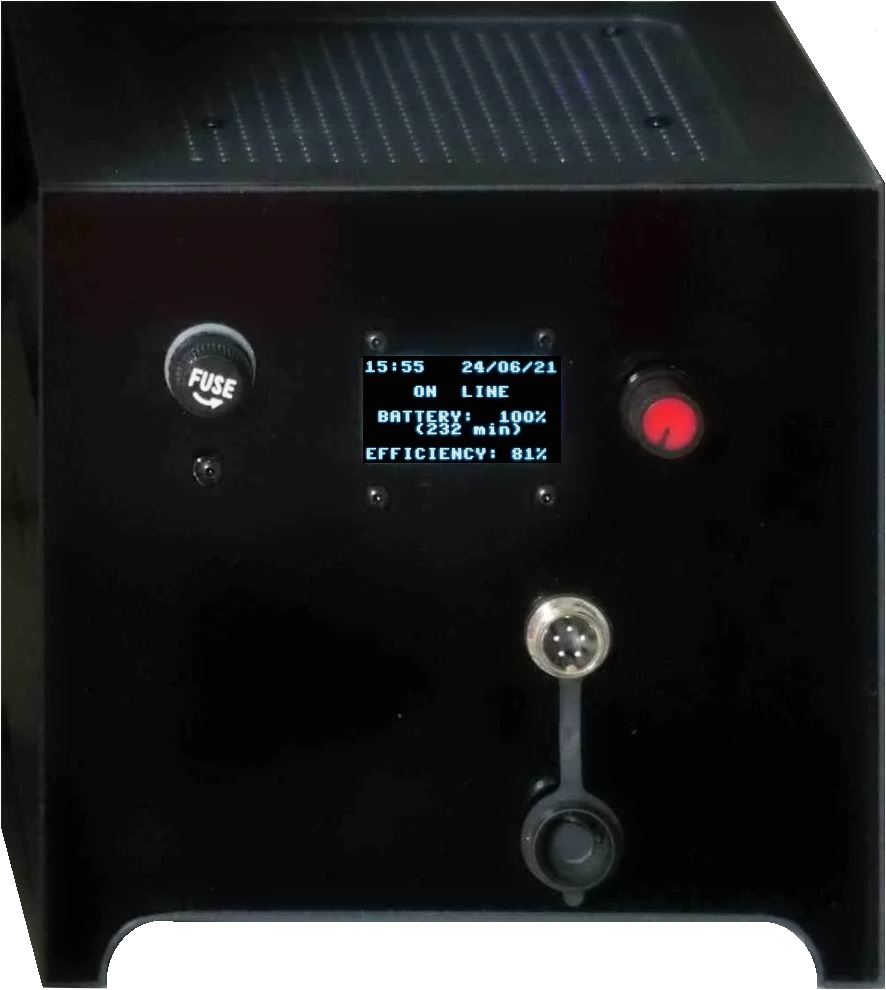
Figure 1. Front view of the DC UPS

The back side of the UPS includes the 220V plug with the power switch, a button to start the UPS when on battery, the serial/USB interface to connect the UPS to the PC or any other client device supporting the APC® UPS-Link protocol (a NAS for example) and obviously the DC power outlets.
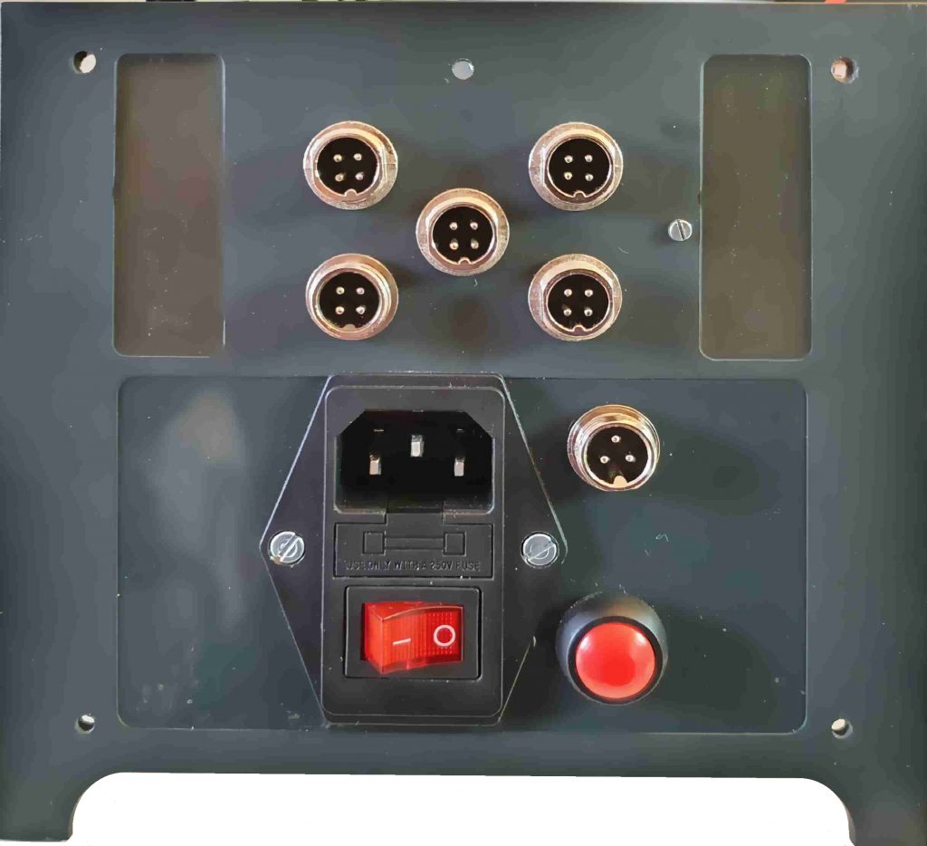
Figure 2. Back view of the DC UPS

Principle of operation

The DC UPS is intended for use with typical low/medium power DC devices like routers, mini pc, monitor, NAS and so on. Differently from a typical AC UPS, that provides an uninterruptible alternate current output, the DC UPS provides a direct current output with different voltage levels as required by connected DC devices. This way, the UPS can be used to power the devices directly replacing the power rectifiers normally used when the devices are connected to the AC plug.
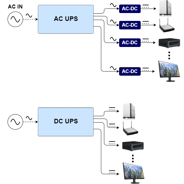
Figure 3. Standard AC-UPS vs. DC-UPS. The DC-UPS eliminates the need of power rectifiers for output devices.

Other than the topology simplification, the AC-UPS and the DC-UPS differ for the number of power conversions being implemented between the AC in plug and the output device. Following picture shows the block diagram of a typical line interactive AC UPS:
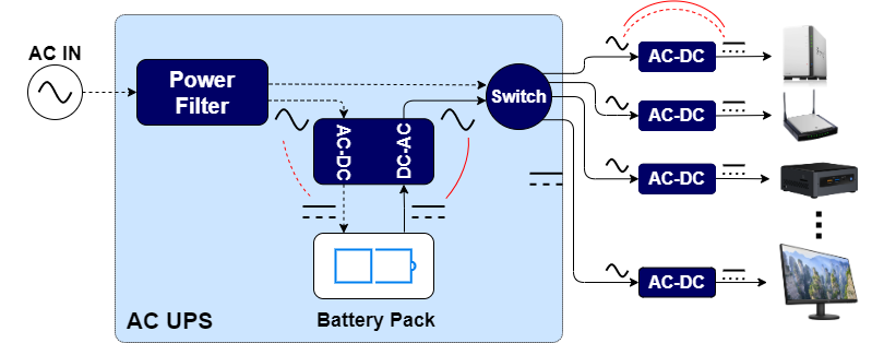
Figure 4. Block diagram of a line interactive AC UPS

Dotted lines represent the connections when the UPS is working on line, while solid lines represent the connections when the UPS is working on batteries. Similarly, red lines highlight the power conversions from AC to DC (rectifiers) and from DC to AC (inverters) in the two cases. As you can see on the diagram, this UPS requires two conversions when on-line, the first one needed to charge the battery (AC-DC rectifier) and the second one needed to convert the UPS output AC power to DC power as required by connected devices (each device having its own power adapter). When the UPS is on batteries you still have two power conversions. The first one from battery DC power to UPS AC output (inverter) and then again the AC to DC conversion by the device power adapters. Nevertheless, the typical output waveform generated these budget UPS is not a pure sine waveform but it more like a square waveform that can be seen as a sine waveform plus a lot of low to high frequencies harmonics representing output noise.

Let’s now have a look to the block diagram of the DC UPS:
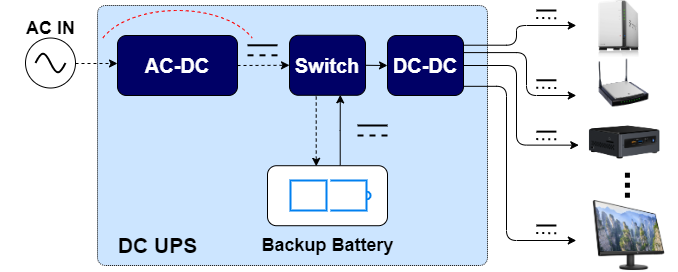
Figure 5. Block diagram of the DC UPS

The topology is quite simpler since it eliminated the need of the inverter and the device power adapters. When working on line you just have one AC to DC power conversion being implemented by the internal SMPS. This generates the stable DC output to charge the battery, and to power the output devices. You only need some additional high efficiency DC to DC regulators (buck/boost converters) to generate the right DC voltage for each device. When working on batteries, there will be no AC/DC or DC/AC conversion in place. The extremely stable battery output will be used to power the output devices.

There are some advantages in using a DC UPS instead of a typical AC UPS, for example:

  • Efficiency:
    • The DC UPS requires less power conversions than the AC UPS thus reducing the power loss in each conversion.
    • One high power, high efficiency SMPS powering all the devices instead of multiple smaller SMPS one for each device. Using one bigger and well-engineered SMPS will allow a better efficiency than using multiple smaller and cheaper power adapters.
  • Battery duration: this is strictly connected to the previous point, considering that when the UPS is on battery only DC-DC power regulators will be working between the battery and the output devices.
  • Space and cabling under the desk.

Solution description

The DC UPS block diagram is the following:
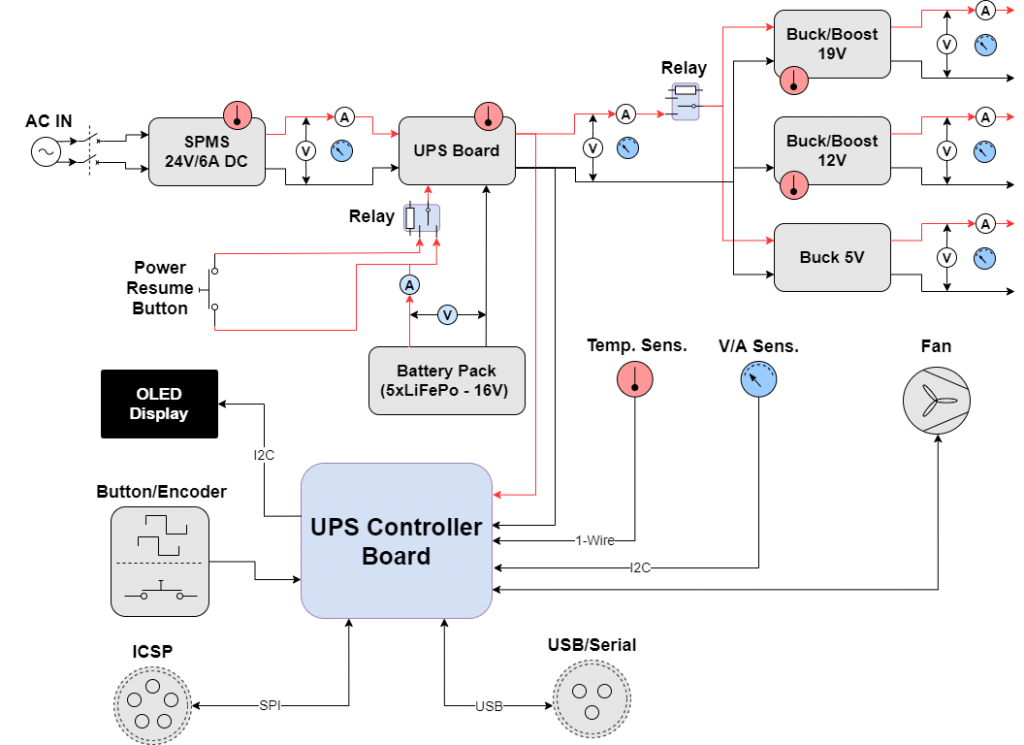
Figure 6. DC UPS block diagram

The AC line is connected to a 24V/6A Swithing Mode Power Supply. The MeanWell LSR 150-24 (see ref. [2]) has been used in this project due to the power provided in a small space. The MeanWell SMPS has a very good efficiency close to 90% and a low profile on only 30mm height.

The output of the SMPS is used to power the DC UPS board (UPS-0528-11 – see ref. [3]). The UPS board is shown in the following picture:
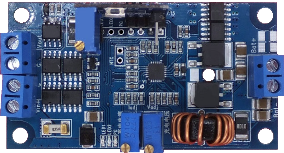
Figure 7. UPS Board

The board is a well-engineered PCB can be found as a preassembled module from different suppliers at a cost between 15 and 20 Euro and delivery from China. Here are the most relevant features:

  • Maximum input current 15A (output current + battery charging current)
  • Unregulated output voltage: this is the input voltage during normal operation or the battery voltage when the input power is missing
  • High efficiency charging with synchronous Step-Down adjustable regulation: both lead acid and lithium batteries are supported
  • Three stage charging: constant current, constant voltage and floating charging
  • Charging cut-off and time limited charging time (after 10 hours of continuous charging – configurable)
  • Minimum power consumption of only 30mA with no load

The backup power storage (backup battery) used for this project is self-made and is based on 5×32700 lithium iron phosphate (LiFePo4) batteries connected in series and packed together. Consequently, the nominal voltage of the battery pack is 16V (5×3.2V) while the limit charging voltage is 18V (5×3.6V). Maximum charging voltage has been limited to 17.3V in this project to preserve battery life while paying a negligible inefficiency in battery capacity. In fact, a typical LiFePo battery gets charged to 99% of its capacity when the charging voltage is between 3.4V and 3.5V that corresponds to something between 17V and 17.5V for our battery pack (see refs. [4] and [5]).

To avoid the batteries to get unbalanced over the time, I have also included a protection module with balancing capability directly into the battery pack. The connection schema between the protection module and the batteries is shown below:
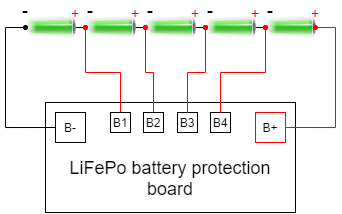
Figure 8. Battery Pack connection schema with protection board

The protection module has the following features:

  • Designed for Lithium Polymer batteries: 3.6-3.7V single cell nominal voltage
  • Single cell battery overcharge protection limit: 4.21-4.29 V
  • Single cell battery over-discharge protection limit: 2.72-2.88 V
  • Over discharge protection current limit: 100A
  • Over temperature protection
  • Shortage protection with 100-600 uS delay
  • Maximum discharge current: 60A
  • Single cell balancing function (60mA charge/discharge balancing current)

The battery pack is connected to the UPS providing the backup power in case of input DC power outage. The UPS board output is not regulated, being the input DC voltage (24V) when on-line and the battery voltage (15-18V) when on battery. The UPS board only ensures that switching between DC input and battery input happens seamlessly in case the power outage. UPS board output is regulated to match the output voltage requirements of the connected devices using buck/boost DC to DC converters. The DC UPS provides three different DC outlets with the following characteristics:

  • Five multiple voltage outlets. Each outlet has four pins. One pin is used for ground the other pins are used to provide different output voltages. This way you can select the output voltage for each outlet just switching the cable. Available output voltages are:
    • 19V/8A
    • 12V/8A
    • 5V/3A

The 19V output requires an automatic buck/boost converter because the UPS board output is higher than 19V when on-line (24V) and lower than 19V when on battery (15-18V). The 12V output would require a buck converter because the UPS board output is always higher than 12V, similarly for the 5V output. Anyway, the same buck/boost converter is used both for 19V and 12V outputs in the latter case leaving the user the possibility to reconfigure the output voltage to a different (possibly higher) value, if necessary.

The buck/boost converter board used for 12V and 19V DC outputs in this project is very popular and in based on the LTC®3780 IC from Analog Devices (see ref. [6]) which is a high-performance automatic buck-boost switching regulator controller that operates from input voltages above, below or equal to the output voltage.
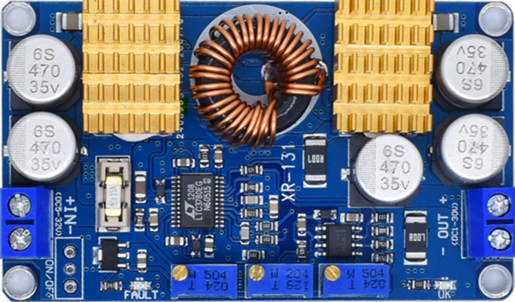
Figure 9. LTC3780 DC-DC automatic buck/boost converter

The converter has the following features (from datasheet):

  • Single Inductor Architecture Allows VIN Above, Below or Equal to VOUT
  • Wide VIN Range: 4V to 36V Operation
  • Synchronous Rectification: Up to 98% Efficiency
  • Current Mode Control
  • +/-1% Output Voltage Accuracy: 0.8V < VOUT < 30V

The buck converter for the 5V output is based on the MH-GX4A DC-DC 4A DC Step-Down regulator which is rated for 4A maximum output current (3A constant output) and a very highconversion efficiency from 24V to 5V that is around 95%. Again, the preassembled module is very cheap and can be easily found on the web.
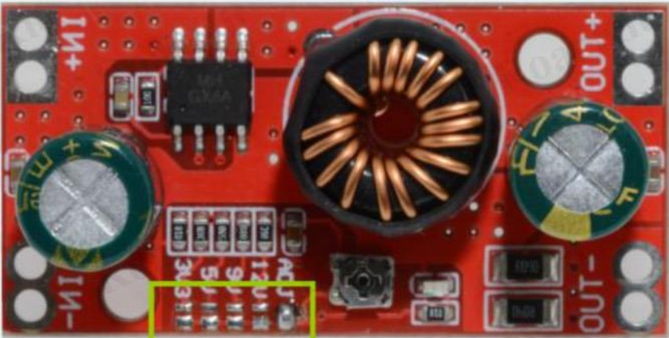
Figure 10. MH-GX4A DC-DC buck converter

The controller board is the core of the project and completes the design. The CPU is the Low-power Atmel® AVR® 8-bit Microcontroller ATmega644p (see ref. [7]). The board includes several external components used to monitor and adjust the UPS operating parameters. The controller board block schema is depicted below:
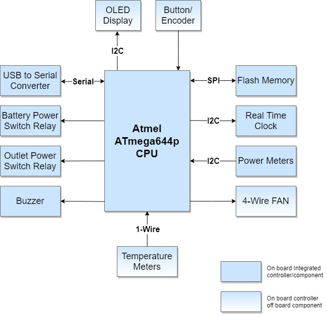
Figure 11. UPS Controller Board block diagram

Details for the diagram components are listed below:

  • Power Meters: these are 6 x I2C INA219A voltage/current sensors (ref. [8]) corresponding to V/A markings on the connection wires in the UPS block diagram (Fig. 6)
  • 4-Wire Fan: this is the fan controller circuit. Fan connection includes both tachymeter and pwm pins respectively to measure and control the fan speed
  • Battery Power Switch Relay: latching power relay (see ref. [9]) driver circuit. This is used to connect/disconnect the battery pack from the UPS board.
  • DC Out Power Switch Relay: latching relay driver circuit. This is to connect/disconnect power for UPS DC outlets. The relay is the same model used for the battery power switch.
  • OLED Display: This is an I2C 128×64 monochrome display
  • Flash Memory: 64Mbit SPI Flash Memory (see ref. [10]) used for UPS data logging
  • Real Time Clock: provides a real time date/time reference to controller board. This is based on the DS3231MZ IC (ref. [11]) and is equipped with a backup battery (CR2032) to keep time when the UPS is shut down
  • Temperature Meters: 1-Wire protocol interface for a chain of 6 x DS18B20 temperature sensors IC (see ref. [12]).
  • Button/Encoder: interface for button / rotary encoder controller circuit. This is used to allow the user to interact with the UPS.
  • USB to Serial Converter: USB interface for UPS state monitoring compatible with APC monitoring protocol
  • Buzzer: a passive buzzer used to send audible alerts to the user when the UPS reaches the low battery condition or in case of critical failures.

Power meters allow the controller software to monitor the global power balance of the UPS and the health status of the DC-DC converters. Sensing both current and voltage enables the software to calculate the total power drain from external devices on the 5V, 12V and 19V outlets. Similarly, power meters located at the UPS board input, output and battery connection can be used to understand whether the UPS is running on batteries or is online and the corresponding power drain from the battery pack or the input power supply. In addition, the control software can monitor if the outlet voltage goes out of the acceptable tolerance and decide to disconnect the output power to protect the external devices. Battery voltage is also used to estimate the state of charge of the battery and, when running on battery, can be used in conjunction with the power drain to calculate the residual life time of the battery. When the residual battery time is below a configured threshold, the UPS starts beeping the buzzer to advice the user to save the current work before the UPS initiates the self-switch off sequence.

The UPS electronic components are mounted on a square iron stand. Components are located on both front and back side of the stand, as shown in the following pictures:
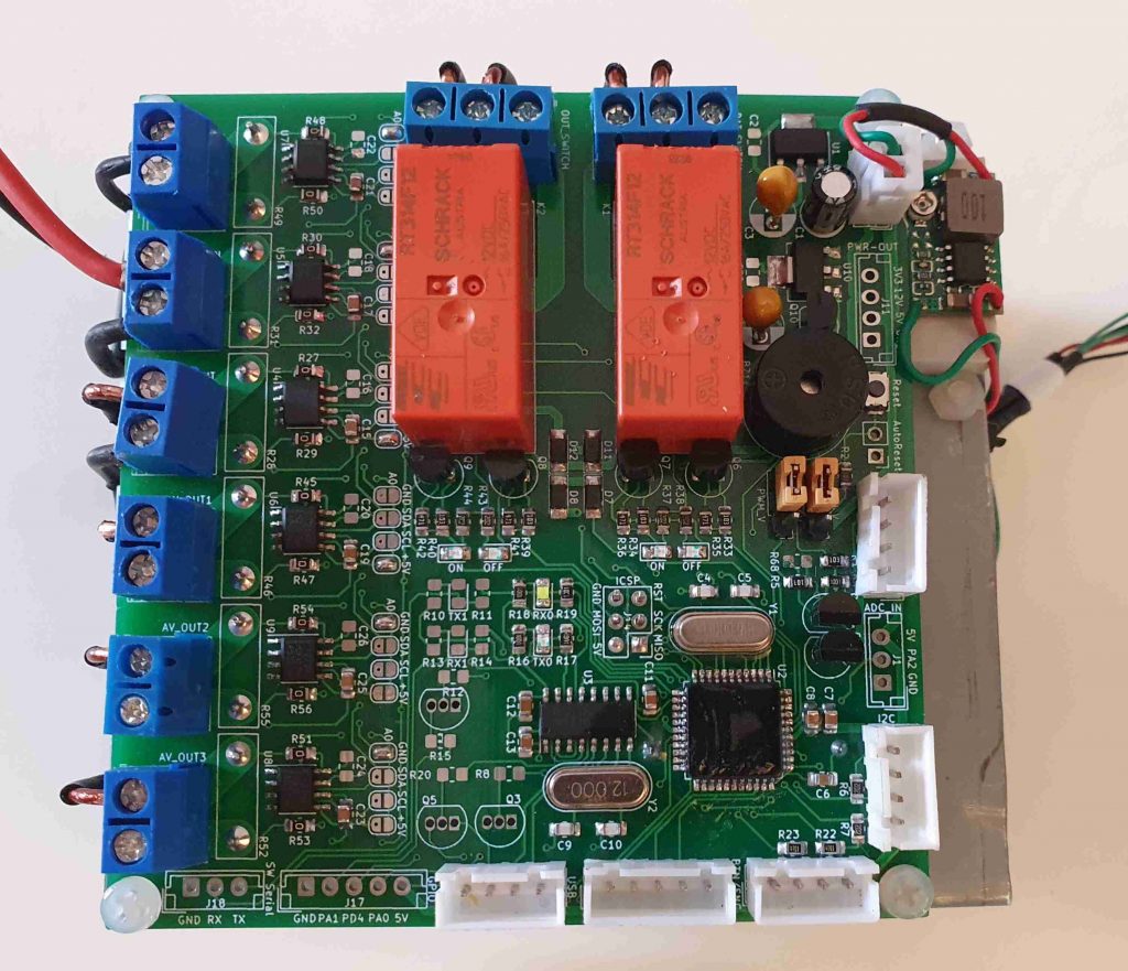
Figure 12. UPS Electronics (front view) – UPS Controller Board PCB

The PCB is mounted on a iron stand which hosts the rest of the components (DC-DC regulators) on the back side, as shown by the following pictures:
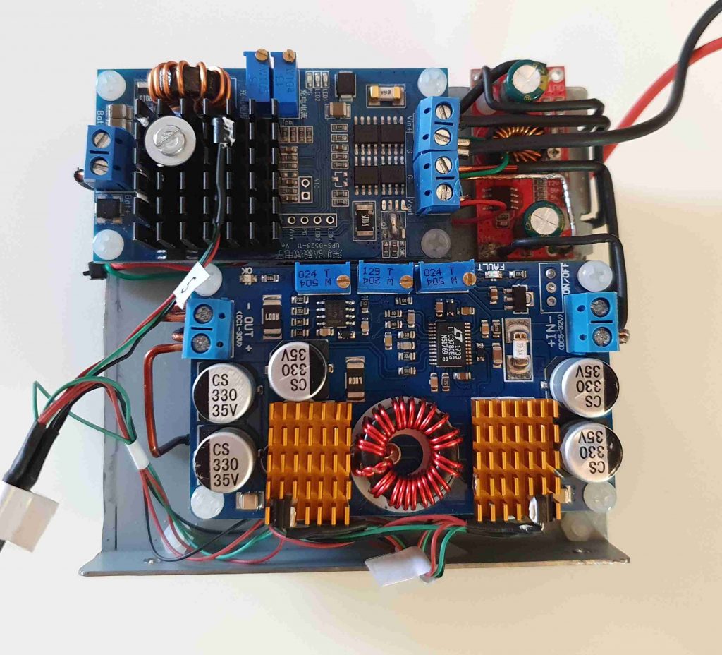
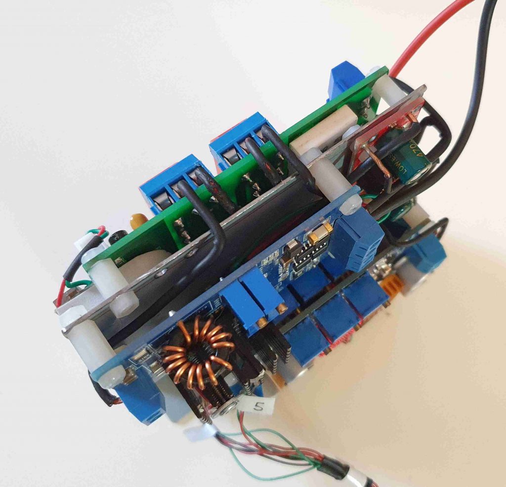
Figure 13. UPS Electronics (back view) – UPS Board and DC-DC regulators
Figure 14. UPS Electronics (upper view)

The housing box of the UPS hosts the SMPS regulator and the UPS electronics as shown in the following picture:
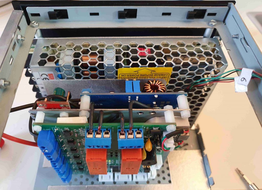
Figure 15. UPS housing box, with SMPS regulator and the electronics components.

The remaining space within the box hosts the battery pack. The front cover of the box hosts the display, the button/encoder, the ICSP programming interface, the back side of the box hosts the DC outlets, the AC input plug, the USB serial interface and the emergency start button (to force restart the UPS on battery). Finally, a low profile cooling fan is mounted just below the lid of the box.

DC UPS Control Software

Other than monitoring the health status of the UPS, the control software is also able to emulate the Smart APC Protocol (see. refs. [13], [14], [15], [16]). In order to use this feature, the device must run the APC monitoring software. In case of a PC, the monitoring software is PowerChute Business Edition (see ref. [17]). The monitoring device must be connected to the UPS using the USB connector located on the back side of the UPS. The USB port is used to emulate a serial port and is operated by the CH340G usb to serial converter (see ref. [18]). Prior to installing the APC software, the CH340G drivers must be installed on the monitoring device (see ref. [19]).

The protocol emulator implements a subset of the APC protocol commands that include both inquiry and configuration commands. When a configuration parameter is changed, the emulation software persists the updated configuration to a permanent storage area (see “Using APC PowerChute management software with DC UPS” section below for more details).

The UPS has an integrated logging service to log events and metrics during operation. Log records are persisted to an external flash storage of 8 Mb (64 mbit) organazed in 2048 pages of 4 Kb each. The logger service stores the records sequentially into the flash storage rolling over the pages when the storage is full.

Log records are quite simple and contain the timestamp, the severity and a short message describing the event. Typical log events include the change of state from “on line” to “on battery” and the “low battery” condition. The timestamp is kept updated by the external RTC clock circuit that includes a small lithium backup battery to hold the time even when the UPS is shut down (both external AC and battery disconnected).

The UPS controller board includes a 1-wire interface to connect a daisy chain of temperature sensors based on the well-known DS18B20 IC. There are six temperature sensors measuring:

  • The SMPS power supply temperature
  • The buck/boost DC-DC regulators temperature (2 sensors each placed on the heat sinks – see figure 9)
  • The UPS board temperature

The controller board software sample the temperature every 10 seconds and calculates the maximum temperature between the monitored components. This is used to regulate the cooling fan speed which is placed just below the upper lid of the case. The target rotation speed in RPM of the fan is a linear function of the maximum temperature.

The algorithm controlling the fan speed is adaptative. Fan interface includes both the speed control line and a tachymeter line to sense the fan rotation speed. The fan speed is regulated by the control software varying the duty cycle of a square wave sent on the speed control line. The square wave must have a fixed frequency that is supposed to be between 25 ad 35Khz to avoid generating audible noise. The actual speed of the fan is sensed through the tachymeter input line and used to adjust the duty cycle in order to reach the target rotation speed. The fan control software implements a closed loop system (see ref. [20]) based on negative feedback control (see ref. [21]) strategy.

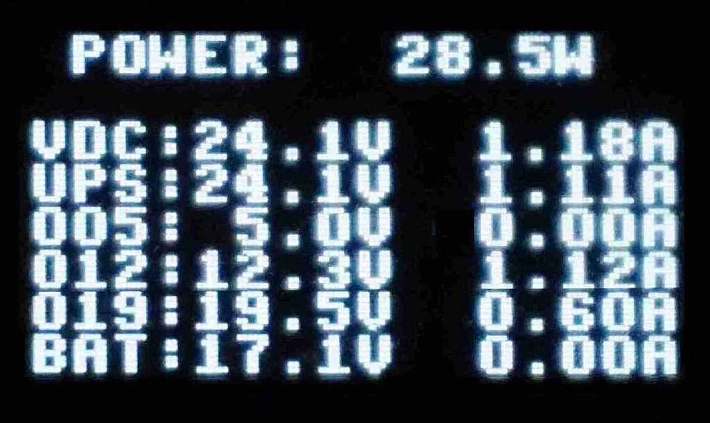
The last element of the design is the I/O subsystem which includes an 128×64 matrix OLED display (see ref. [22]) based on the well-known SSD1306 driver IC (see ref. [23]) and a rotary encoder with a button. Display is used to show the operating parameters of the UPS like the status, the battery level, the total efficiency, the output voltage, current and power and the system logs. Using the encoder and the integrated button, the user interacts with the UPS control software to browse different pages of the display, adjust the time or switch off the UPS.

Following picture shows sample pages of the UPS display:
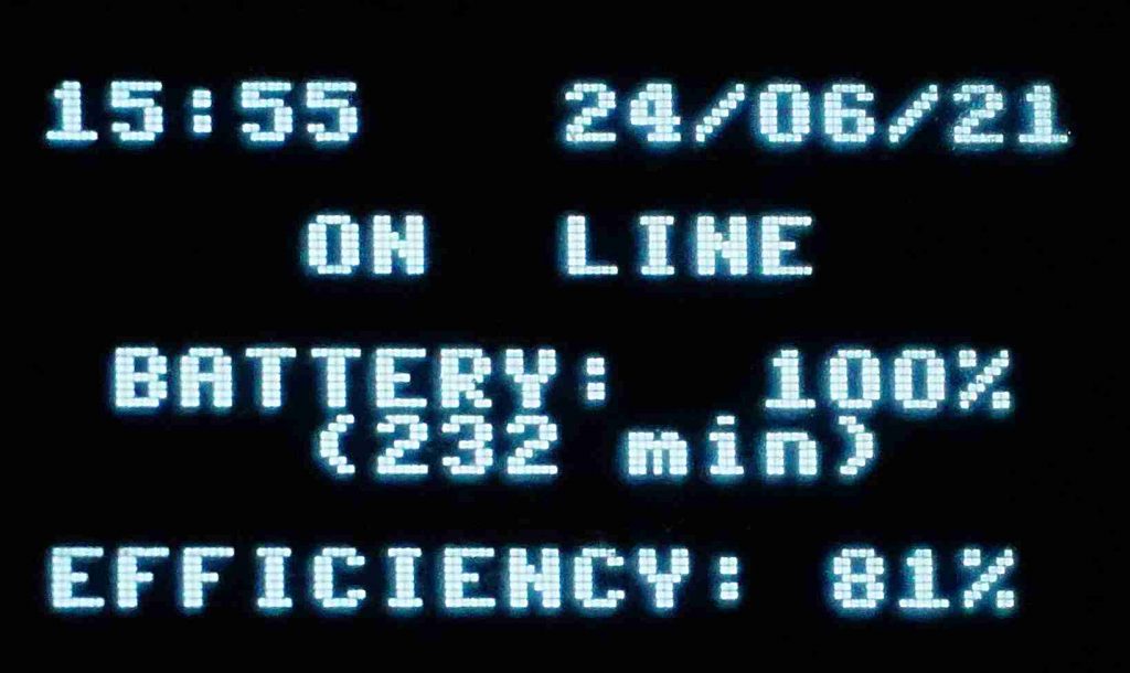
Figure 16. UPS Main Page
Figure 17. UPS Power Monitoring Page

Using APC PowerChute management software with DC UPS

As briefly introduced above, the UPS control software is able to emulate the APC® UPS-Link protocol to provide information about UPS status, the battery level, the estimated remaing runtime remaining when on battery and so on. On a Linux or Windows PC connected to the UPS the utility understanding the UPS-Link protocol is PowerChute Business Edition. This utility, installs a background agent running on the PC that communicates with the UPS and can be configured to execute the proper actions when the UPS is on battery or is low of battery. Examples of these actions include running a custom command or/and hibernate/shutdown the PC. The UPS Link protocol is a serial protocol running at 2400 bps. As shown in figure 2, on the back side of the DC UPS there is a USB connector. This is a serial over USB channel handled by the CH340G processor. After installing the proper drivers on the client device, the USB connection is recognized as a standard COM serial port on the client device.

During the installation process PowerChute Business Edition (PBE) requires the user to set the target UPS model. To make sure the PBE agent will use the UPS Link protocol, a possibility is to select “Other type B” as UPS model and the COM interface corresponding to the UPS connection as serial port. The software will install an agent that, on a Windows machine corresponds to a service named “APC PBE agent”. The service will be shown in the Windows service list dialog with the following name and description:

Figure 14. PowerChute Business Edition service on Windows

The agent has a web interface that can be accessed at the following URL:

https://localhost:6547

If the agent is running, the following login screen should appear:

Figure 18. PowerChute Business Edition login form

After logging in with the credential entered during the installation process, if the connection between the agent and UPS is ok, the main page will display UPS properties, like the following:
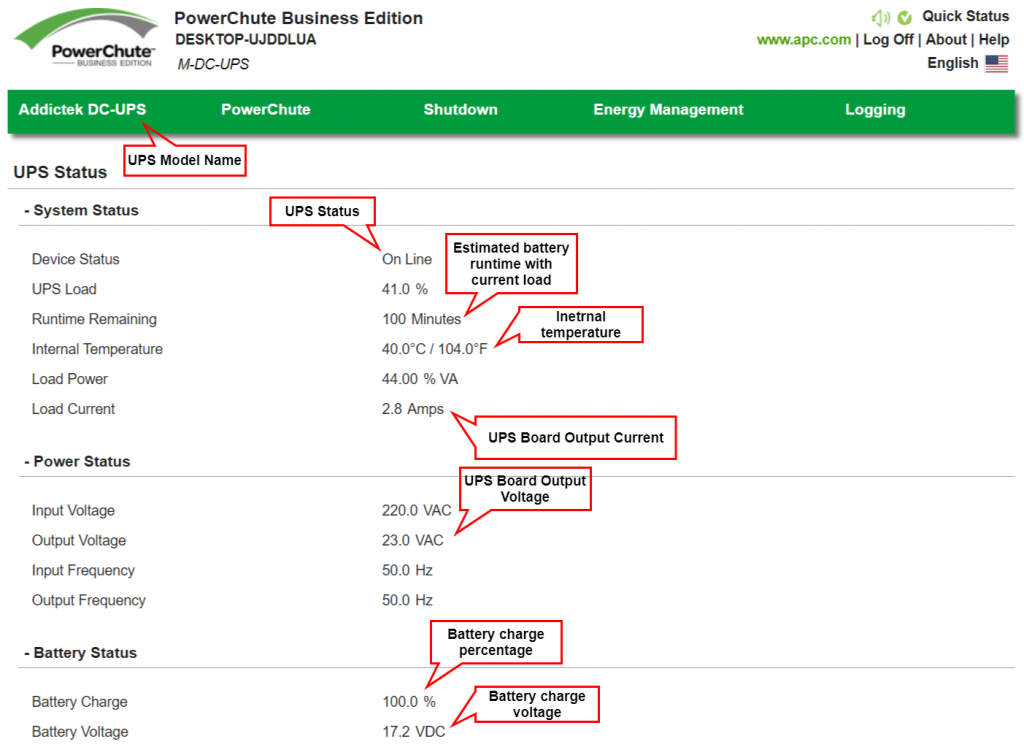
Figure 19. PowerChute Business Edition main page

The rest of the pages allow the user to configure the agent behavior, like the shutdown process when the UPS gets on battery/low battery.

References

[1] Lady Ada Adafruit -. Industries. Power Capacity and Power Capability. , Jun 25, 2021.
[Bibtex]
@battery_power{battery_power,
author="Lady Ada - Adafruit Industries",
title = "{Power Capacity and Power Capability}",
year = "Jun 25, 2021"
}
[2] MeanWell. LSR-150-24 – 150W Single Output Switching Power Supply. , 2021.
[Bibtex]
@mw_lsr_150_24{mw_lsr_150_24,
author = "MeanWell",
title = "{LSR-150-24 - 150W Single Output Switching Power Supply}",
year = "2021"
}
[3] Unknown. High power dc ups module [Bibtex]
@ups_0528_11{ups_0528_11,
author = "Unknown",
title = "High Power DC UPS Module}
[4] PowerStream. How does capacity correlate with charge voltage for lithium iron phosphate batteries?. , Apr 23, 2021.
[Bibtex]
@lifepo4_1{lifepo4_1,
author = "PowerStream",
title = "{How does capacity correlate with charge voltage for lithium iron phosphate batteries?}",
year = "Apr 23, 2021"
}
[5] PowerStream. How to charge Lithium Iron Phosphate Rechargeable Lithium Ion Batteries. , Jul 31, 2019.
[Bibtex]
@lifepo4_2{lifepo4_2,
author = "PowerStream",
title = "{How to charge Lithium Iron Phosphate Rechargeable Lithium Ion Batteries}",
year = "Jul 31, 2019"
}
[6] Analog Devices. LTC3780 – High Efficiency, Synchronous, 4-Switch Buck-Boost Controller. , Feb 2019 – Rev. G.
[Bibtex]
@ltc3780{ltc3780,
author = "Analog Devices",
title = "{LTC3780 - High Efficiency, Synchronous, 4-Switch Buck-Boost Controller}",
year = "Feb 2019 - Rev. G"
}
[7] Atmel Corporation. ATmega644P – 8-bit AVR Microcontroller with 64K Bytes In-System Programmable Flash. , 2015.
[Bibtex]
@atmega644p{atmega644p,
author = "Atmel Corporation",
title = "{ATmega644P - 8-bit AVR Microcontroller with 64K Bytes In-System Programmable Flash}",
year = "2015"
}
[8] Texas Instruments. INA219 Zerø-Drift, Bidirectional Current/Power Monitor With I2C Interface. , Aug 2008 – Rev. Dec. 2015.
[Bibtex]
@ina219a{ina219a,
author = "Texas Instruments",
title = "{INA219 Zerø-Drift, Bidirectional Current/Power Monitor With I2C Interface}",
year = "Aug 2008 – Rev. Dec. 2015"
}
[9] Schrack. 16A Bistable Power PCB Relay. , Aug 2019, Rev. 0819.
[Bibtex]
@rt314f12{rt314f12,
author = "Schrack",
title = "{16A Bistable Power PCB Relay}",
year = "Aug 2019, Rev. 0819"
}
[10] Winbond. W25Q64FV – 3V 64M-BIT SERIAL FLASH MEMORY WITH DUAL/QUAD SPI & QPI. , Jul 18, Rev. S.
[Bibtex]
@w25q64fv{w25q64fv,
author = "Winbond",
title = "{W25Q64FV - 3V 64M-BIT SERIAL FLASH MEMORY WITH DUAL/QUAD SPI & QPI}",
year = "Jul 18, Rev. S"
}
[11] Maxim Integrated. DS3231 – Extremely Accurate I2C-Integrated RTC/TCXO/Crystal. , 19-5170; Rev 10; 3/15.
[Bibtex]
@ds3231mz{ds3231mz,
author = "Maxim Integrated",
title = "{DS3231 - Extremely Accurate I2C-Integrated RTC/TCXO/Crystal}",
year = "19-5170; Rev 10; 3/15"
}
[12] Maxim Integrated. Programmable Resolution 1-Wire Digital Thermometer. , 19-7487; Rev 6; 7/19.
[Bibtex]
@ds18b20{ds18b20,
author="Maxim Integrated",
title = "{Programmable Resolution 1-Wire Digital Thermometer}",
year = "19-7487; Rev 6; 7/19"
}
[13] Schneider-Electric. APC by Schneider Electric UPS-Link Communications Protocol Specification. , 2019.
[Bibtex]
@apc_smart_protocol{apc_smart_protocol,
author = "Schneider-Electric",
title = "{APC by Schneider Electric UPS-Link Communications Protocol Specification}",
year = "2019"
}
[14] Network UPS Tools. APC’s smart protocol. , Sep. 2016.
[Bibtex]
@apc_smart_protocol_1{apc_smart_protocol_1,
author="Network UPS Tools",
title = "{APC’s smart protocol}",
year = "Sep. 2016"
}
[15] Kiryl Bahdanau. Unofficial APC UPS protocol. , Feb. 2020.
[Bibtex]
@apc_smart_protocol_2{apc_smart_protocol_2,
author="Kiryl Bahdanau",
title = "{Unofficial APC UPS protocol}",
year = "Feb. 2020"
}
[16] Various. APC’s smart protocol. , Feb. 2000.
[Bibtex]
@apc_smart_protocol_3{apc_smart_protocol_3,
author="Various",
title = "{APC’s smart protocol}",
year = "Feb. 2000"
}
[17] Schneider-Electric. APC – PowerChute Business Edition. , v10.0.2 – 2021.
[Bibtex]
@apc_powerchute_be{apc_powerchute_be,
author="Schneider-Electric",
title = "{APC - PowerChute Business Edition}",
year = "v10.0.2 - 2021"
}
[18] Ltd. Nanjing Qinheng Microelectronics Co.. CH340 – USB to UART Bridge Controller. , N/A.
[Bibtex]
@ch340g{ch340g,
author="Nanjing Qinheng Microelectronics Co., Ltd.",
title = "{CH340 - USB to UART Bridge Controller}",
year = "N/A"
}
[19] Ltd. Nanjing Qinheng Microelectronics Co.. CH340 – Drivers Download. , N/A.
[Bibtex]
@ch340g_drivers{ch340g_drivers,
author="Nanjing Qinheng Microelectronics Co., Ltd.",
title = "{CH340 - Drivers Download}",
year = "N/A"
}
[20] Electronics Tutorials. Closed-loop Systems. , Jan. 2019.
[Bibtex]
@closed_loop_systems_1{closed_loop_systems_1,
author="Electronics Tutorials",
title = "{Closed-loop Systems}",
year = "Jan. 2019"
}
[21] Electronics Tutorials. Negative Feedback Systems. , Sep. 2019.
[Bibtex]
@negative_feedback_systems_1{negative_feedback_systems_1,
author="Electronics Tutorials",
title = "{Negative Feedback Systems}",
year = "Sep. 2019"
}
[22] Vishay. I2C 128×64 Graphic OLED Display. , Sep. 2019.
[Bibtex]
@oled128x64{oled128x64,
author="Vishay",
title = "{I2C 128x64 Graphic OLED Display}",
year = "Sep. 2019"
}
[23] Solomon Systech. 128×64, Dot Matrix OLED/PLED Segment/Common Driver with Controller. , Sep. 2019.
[Bibtex]
@ssd1306{ssd1306,
author="Solomon Systech",
title = "{128x64, Dot Matrix OLED/PLED Segment/Common Driver with Controller}",
year = "Sep. 2019"
}
WiFi Programmable Thermostat


Introduction

The goal of this project was enabling smart management of my home comfort from anywhere. This is monitoring or adjusting heating temperatures via computer, smartphone or tablet, so being able to check the heating status, change target temperature or the daily and weekly programming using a user-friendly interface. A secondary, but equally important goal of the project was the thermostat exterior design and the solution engineering. I wanted the electronic circuit to fit the size of a masonry wall box and the human interface (display and commands) to fit the shape and the size of some civil series. The final result is the following:

Project components

The thermostat is based on the well-known ESP8266 which includes a built-in Wi-Fi controller and very good computational capabilities with 80Mhz clock CPU, 80Kb of RAM and 4Mb flash storage for program code and data.

The project hardware includes a sensor to monitor ambient temperature and humidity) and a subminiature power latching relay to switch heating on or off.

The thermostat human interface includes a small 1.3″ OLED display to show the basic information like temperature, humidity, working mode and status. A small 5-way joystick is used to interact with the thermostat local interface for example to change the working mode and modify various thermostat configuration options.

A small SMPS provides the regulated 3.3v source required to operate the ESP8266 and all the other components.

Other than the local interface, the thermostat can be monitored and configured remotely using a web application interface. Advanced configuration options like changing the daily and weekly temperature programming are only available using the web interface.

Thermostat block diagram

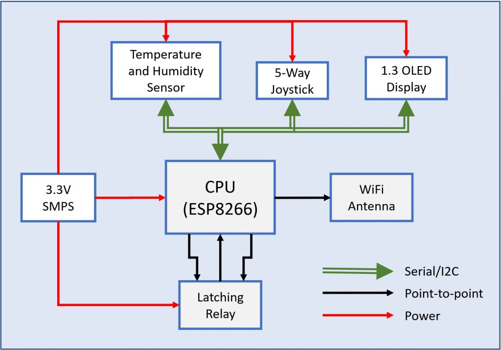
Following picture shows the thermostat block diagram:

The I2C bus connects the temperature/humidity sensor, the OLED display and the 5-way joystick to the CPU. The latching relay is connected directly to the CPU using two control pins (to switch the relay contact ON or OFF – double coil relay) and a feedback pin. The feedback pin is used to check the relay status at system startup and verify that the latching relay contact is switched on the correct position (see “Latching Relay Status Feedback Management” section later on for details).

The thermostat features are the following:

  • Operating mode:
    • Auto: the thermostat automatically switches the heating system on or off comparing the ambient temperature and the target temperature set by the user.
    • Away: the thermostat normal status is off but it switches on the heating system if ambient temperature goes below the freezing temperature which is set to 5 degrees Celsius.
    • Cleaning: the thermostat switches off for 3 hours from the moment this mode is activated and then reverts back to the Auto mode. This is especially useful to avoid the heating system to switch on in winter time when opening windows during housekeeping time.
    • Manual: the thermostat is activated manually setting the target temperature to the desired value.
    • Off: the thermostat is switched off.

When is Auto mode, the target temperature is set according to a program of the day which defines the target temperature with a resolution of 30 minutes. There are up to three different programs that can be set and associated with the days of the week. Usually, just two programs are used one for Monday to Tuesday and the second program for the weekend. A third program is available for different needs.

User interface

The thermostat is connected to internet through the home Wi-Fi connection. Programming the thermostat can be done either by the local interface (thermostat joystick on the right hand side of the display) or the remote web interface. The local interface allows the user to switch between the different operating modes and change main settings of the thermostat. The web interface allows the user to monitor the thermostat status, change the operating mode or modify the weekly programming used by the Auto mode. Web interface interaction with the thermostat make use of the long polling technique (see “Remote Interface Interaction” section below for details).

Some features are only avaliable by the local or remote interface, here is the list:

FeatureLocal InterfaceWeb Interface
Change operating modeXX
Set target temperature in manual modeXX
Change weekly programsX
Associate Weekly program to DaysX
Adjust thermostat internal configuration parametersX
Monitor ambient temperatureXX
Monitor ambient humidityX
Advanced monitoring of temperature/humidity history (day/week/month/year)X
Set target end of time in cleaning modeXX
Table 1. Local vs. Web Interface

The local interface has two pages:

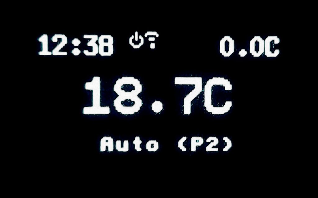
  • Main screen: here you have the time on the upper left corner, then some icons showing the heating status (on/off), the Wi-Fi connection status. The target temperature is on the upper right corner while current temperature is at the center of the display. Finally, on the bottom you can see the operating mode.
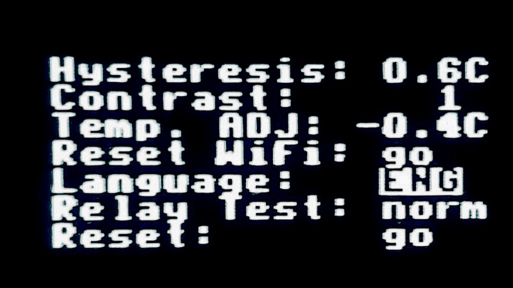
  • Settings screen: here you can change the internal configuration of the thermostat. These include:
    • Hysteresis: this is the minimum difference between the target temperature and current temperature that must exist to switch heating on again after the target temperature has been reached.
    • Contrast: the display brightness
    • Temp. ADJ: this is the temperature adjustment offset from -2 to 2 degrees Celsius used for temperature sensor fine tuning.
    • Reset WiFi: to restart Wi-Fi and put the thermostat in hotspot mode. This way, you can connect a smartphone or tablet to the thermostat and enter Wi-Fi connection parameters (ssid, key).
    • Language: the local and remote interface display language. English and Italian are supported, more to come.
    • Relay Test: used to force the heating relay on or off for testing purposes.
    • Reset: to restart the thermostat.

To enter the settings page from the main page you need to keep the joystick button pressed for more than 3 seconds.

On the settings page you can browse the configuration options up and down using the joystick. Once you have selected the desired option you can enter into the change mode moving the joystick in the right direction. When the option value is highlighted you can change its value moving the joystick up and down. To leave the change mode just move the joystick in the left direction.

To go back to the main page keep the joystick pressed again for more than 3 seconds.

Here are the screenshots of the display pages:

Main display page
Settings display page

The web interface has three tabs:

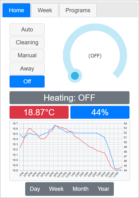
  • Home: here you can set the operating mode, check ambient temperature and humidity, explore their trend through an interactive graph (pan/zoom) over the last day/week/month/year
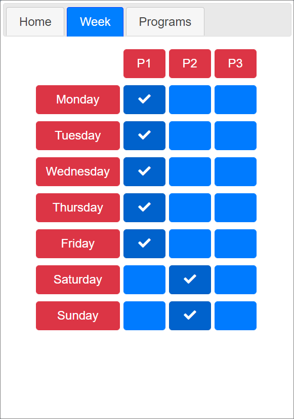
  • Week: here you can switch the program associated to the days of the week
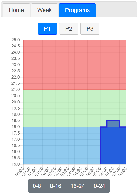
  • Programs: here you can change the daily program setting the desired temperature for each time of the day. You can set up to three programs and the time resolutiin is 30 minutes.

Here are the screenshots of the tabs:

Home tab

The operating mode is selected using the button on the upper left side. When the operating mode is manual, the slider can be used to set the target temperature.

On the center of the page you have the heating status (on/off) and ambient temperature and humidity. On the bottom of the page, the temperature and humidity graph is interactive. You can select the reference period using the button below the graph and then pan and zoom on the time axis to refine the analysis window.

Week tab

The week tab is very simple you can select the program applied to each day of the week.

Programs tab

On the top of the page you can select the program to be configured. The bar graph allow you to set the target temperature at every time of the day. You can focus a specific period of the day using the buttons below the graph, then you can pan and zoom on the time axis to focus on specific hours of the day. Finally, clicking on the graph you can adjust the target temperature.

Thermostat internals

The thermostat is composed by the controller board, the i/o board which embeds the temperature and humidity sensor and the OLED display.

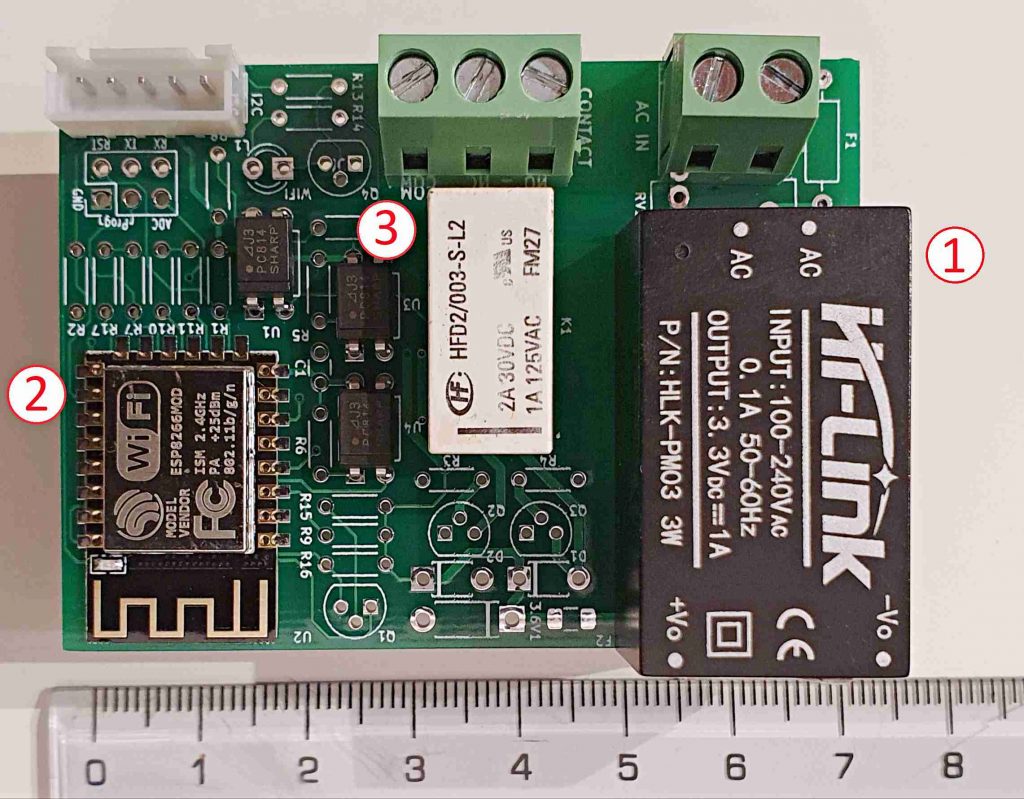
Following picture shows the main board in a early stage of the assembly. The size of the board is 68mm x 48mm:

Main components of the board are the (1) AC-DC SMPS converter (Hi-Link HLK-PM03 – see ref. [1]) that provides 3.3v regulated output, (2) the ESP 12-F WiFi module based on ESP8266 CPU (see ref. [2]) and (3) the latching relay that provides NO/NC contacts to switch the heating system on or off.

Latching relay is the subminiature dip relay HFD2-003-S-L2 (see ref. [3]) which has double coil and a nominal voltage of 3v. It can switch 125Vac/1A resistive load while the maximum rating is 220Vac/250Vdc at 3A. This is more than enough to drive typical heating system switching contact that is usually either a mechanical or solid-state relay. This latching relay offers two contacts, the second one is used to check the status of the relay and detect possible switching failures.

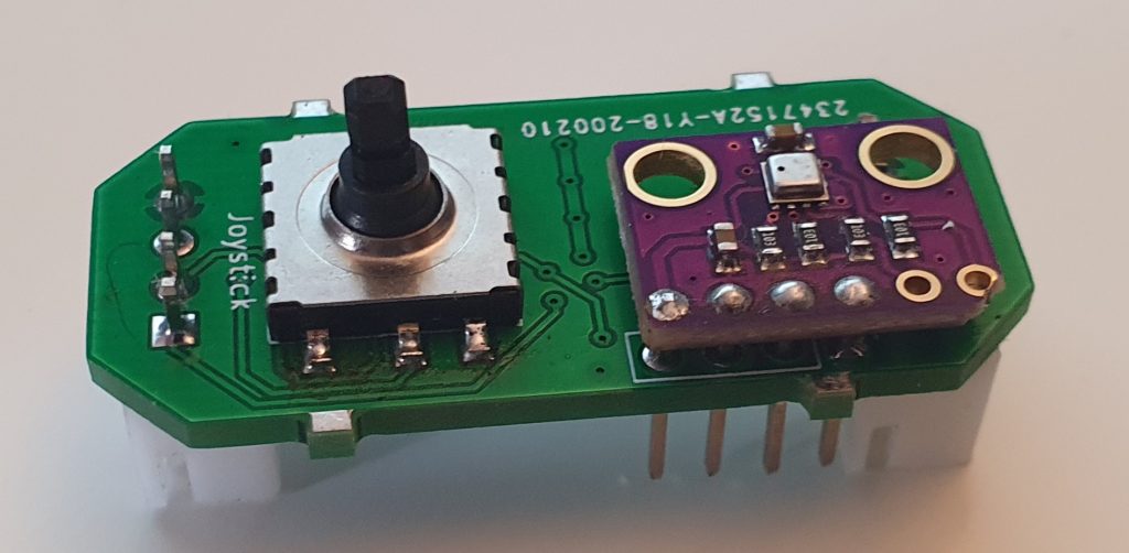
The I/O interface is composed by the joystick and the temperature sensor. This is connected to the main board using the I2C interface. The joystick has five contacts, one for the push button and four for the move directions. The joystick contacts are connected to the I2C bus using PCF8574 Remote 8-Bit I/O Expander (see ref. [4]). The temperature sensor is the well-known Bosh BME280 (see ref. [5]) which provides a native I2C bus connection. Here is a picture of the I/O board.

I/O board front view
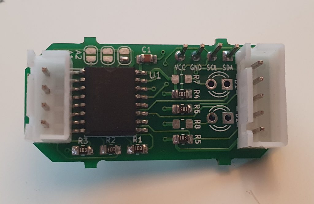
I/O board back view

The back side of the board hosts the PCF8574 IC and two I2C connectors, one is used to connect the I2C bus to the main board and the other one is used as I2C bridge to the OLED display. Please, note that the I2C connector to the main board has an additional interrupt pin to notify a change of the joystick status and avoid polling for I/O changes. This is provided directly by the PCF8574 IC.

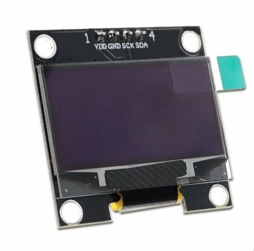
Finally, the display is an 1.3″ monochrome OLED with I2C bus interface based on SSD1306 IC (see ref. [6]) that can be found for a few coins on many e-commerce sites:

1.3″ Monocrome OLED display

Remote Web Interface and local interface Interaction

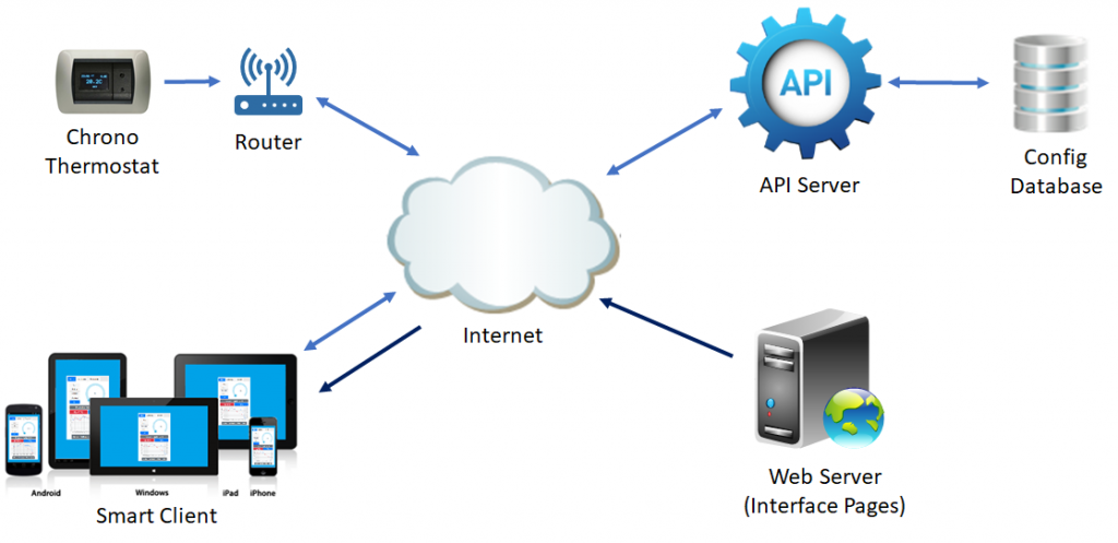
Following diagram shows the interconnections between a remote web interface (operated by the Smart Client), the local thermostat interface and the central components (API Server, Web Server and configuration database):

The pages of the remote web interface are provided by the Web Server. The API Server exposes web services to update the thermostat configuration parameters, read the current configuration and poll for configuration changes. Configuration is stored both remotely in the configuration database and in the local thermostat flash storage. Web pages downloaded bu the Smart Client embed the JavaScript code that interact with API Server to read the current configuration, check for configuration changes or update the configuration in case the user changes thermostat parameters (e.g. the operating mode or the target temperature). Configuration changes can be originated either from the Smart Client via the web interface or from the Chrono Thermostat via the local interface. In both cases, the new configuration is first sent via the API Server to the configuration database and then propagated to the other party.

To check for configuration changes both the remote web interface and the thermostat local interface make use of the Long Polling technique. Basically, the client makes an asynchronous call to the API Server which lasts up to 10 seconds (maximum polling interval). In case the configuration doesn’t change during the polling interval, a “no configuration change” response code is sent to the client at the end of the interval. If a configuration change is detected during the polling interval a “configuration changed” is immediately returned to the client along with the new configuration. This way, the frequency of the polling is highly reduced with respect to the continuous polling techniques (in case of no configuration changes, the frequency will be 6 pools for minute with 10 seconds polling interval), while the client is notified almost immediately when the configuration changes.

Next Steps

Possible evolutions of this project include:

  • Using Web Sockets in place of Long Polling for remote interface interaction will remove the need of the central configuration database. In this scenario, the remote interface would interact directly with the thermostat.
  • Adding a 868/433Mhz radio module (e.g. LoRa Ra-02 or similar) would allow the thermostat to act as a central hub for peripheral automation modules. For example, controlling thermal actuators, additional temperature/humidity monitoring devices, irrigation valves, and so on. Using low power radio will allow the peripheral devices to be battery powered.
  • At present, the thermostat retrieves current time from NTP servers once it is connected to internet. It does not startup until current time is set. In case of temporary power outage, if the internet connection is not reestablished, the thermostat will not work. Adding a RTC (Real Time Clock) module with a backup battery to keep time synchronized would solve this problem.
  • In addition to multi-language support, it would be useful adding some localization features like Celsius vs. Fahrenheit and different time formats

References

[1] HiLink. HLK-PM03 3.3V 3W Power module description and Datasheet. , 2020 rev. 1.01.
[Bibtex]
@hlk_pm03{hlk_pm03,
author = "HiLink",
title = "{HLK-PM03 3.3V 3W Power module description and Datasheet}",
year = "2020 rev. 1.01"
}
[2] Ai-Thinker Technology. ESP-12F WiFi module. , 2018.
[Bibtex]
@hlk_pm03{esp_12f,
author = "Ai-Thinker Technology",
title = "{ESP-12F WiFi module}",
year = "2018"
}
[3] HONGFA. HFD2 Subiminiature DIP Relay. , 2020 rev. 1.01.
[Bibtex]
@hfd2_003_S_L2{hfd2_003_S_L2,
author = "HONGFA",
title = "{HFD2 Subiminiature DIP Relay}",
year = "2020 rev. 1.01"
}
[4] Texas Instruments. PCF8574 Remote 8-Bit I/O Expander for I2C-Bus. , 2015 rev. J.
[Bibtex]
@pcf8574{pcf8574,
author = "Texas Instruments",
title = "{PCF8574 Remote 8-Bit I/O Expander for I2C-Bus}",
year = "2015 rev. J"
}
[5] Bosch. BME280 Combined humidity and pressure sensor. , 2018 rev. 1.6.
[Bibtex]
@bme280{bme280,
author = "Bosch",
title = "{BME280 Combined humidity and pressure sensor}",
year = "2018 rev. 1.6"
}
[6] Solomon Systech. 128×64, Dot Matrix OLED/PLED Segment/Common Driver with Controller. , Sep. 2019.
[Bibtex]
@ssd1306{ssd1306,
author="Solomon Systech",
title = "{128x64, Dot Matrix OLED/PLED Segment/Common Driver with Controller}",
year = "Sep. 2019"
}
Solar Heating Controller

It is a solution for the integrated management of a solar thermal system and a gas boiler for the production of domestic hot water. It allows you to optimally manage the flow of hot water produced by the solar thermal panels, to limit or exclude the intervention of the gas boiler in the summer time and use the gas boiler just to integrate the thermal panels when the solar radiation is not enough to guarantee the minimum temperature required for the consumption of sanitary water. It is composed by a sensor, positioned near the solar tank, which measures the water temperature and transmits it to a central unit located near the gas boiler. The central unit, depending on the exchange temperature configured by the user, decides whether to deviate the flow of hot water from the solar tank directly to the sanitary consumption or send it through the boiler to integrate the thermal energy and therefore the water temperature at the desired level. A three-way valve is used to deviate the flow of the water and works in two positions:

  • Bypass position: when the temperature of the solar storage tank is higher than the exchange temperature, the flow of hot water from the solar tank “bypasses” the boiler which remains inactive for the production of sanitary water
  • Integration position: when the temperature of the solar storage tank is lower than the exchange temperature, the flow of water (preheated) coming from the solar tank is passed through the boiler which raises the water temperature to the desired level.

The sensor is powered by a solar cell and a backup battery and transmits data to the central unit via radio at the frequency of 433Mhz.

The central unit controls the exchange valve and decides the direction of the hot water flow comparing the temperature of the water in the solar tank received by the sensor and the exchange temperature configured by the user.

In addition, the central unit collects external environmental information such as temperature and humidity and checks the filling status of the tank used to collect the condensate produced by the gas boiler (in case of condensing boilers without free drain).

The central unit can be connected to the home WiFi network to transmit the system operating information to the Internet for remote monitoring purposes.

Sensor

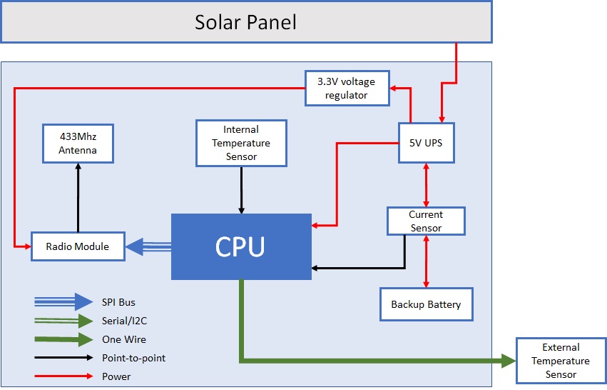
Here follows the block diagram of the sensor:

Sensor block diagram

Diagram includes:

  • Central Processing Unit (CPU)
  • 433Mhz radio communication module with antenna
  • External temperature sensor (to measure the water temperature in the tank)
  • Internal temperature sensor
  • Battery current and voltage sensor
  • Backup battery
  • 5v regulated output UPS module
  • 3.3v voltage regulator

The sensor is hosted inside a waterproof box with a transparent cover. A photo voltaic module is placed just below the cover and generates the electricity required by the electronic board. A UPS module and a backup battery complete the power supply section to ensure that the sensor can continue to transmit data for several days even in the absence of sufficient solar radiation.

The temperature of the water in the solar tank is measured by a probe based on the Dallas DS18B20 sensor.

The temperature data as well as other internal operating parameters of the sensor (battery level, charge / discharge current, internal temperature of the box), are transmitted to the central unit using the radio module with a transmission frequency of 433Mhz.

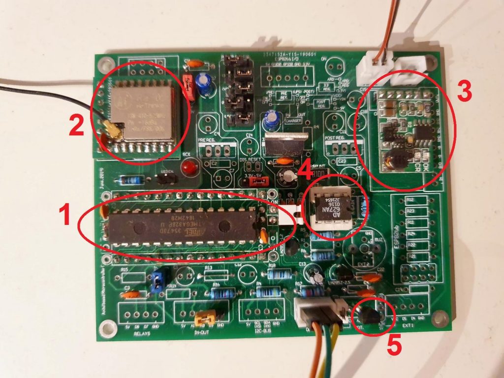
The following figure shows the sensor electronic board.

The component (1) is the heart of the board and is based on the Atmel ATmega328p microcontroller produced by Microchip Technology (ref. [1]). The component (2) is the LoRa Ra-02 data transmission module produced by AI-Thinker and based on the SX1278 chip (ref. [2]) working at the frequency of 433MHz. The component (3) is the UPS module connected to the photo voltaic module and to the backup battery, providing the 5V regulated power source required by the electronic board.

The board is also equipped with two optional components: the first (4) is an instrumental amplifier used to measure the current flowing to and from the backup battery. Current intensity and direction are used to to determine the State of Charge (SoC) of the backup battery. The intensity of the battery charge current is also a good indicator of the intensity of solar radiation and can be used for environmental monitoring. The second optional component is a temperature sensor, based on the MCP9700 active thermistor produced by Microchip Technology (ref. [4]) that can measure temperature in a wide range going from -40 to 125 ° C with good accuracy in the typical operating range of this device (-10 to 50 ° C). This sensor is used to measure the internal temperature of the box hosting the electronic components to check the operating limits and adjust the sensor operating parameters according to the temperature.

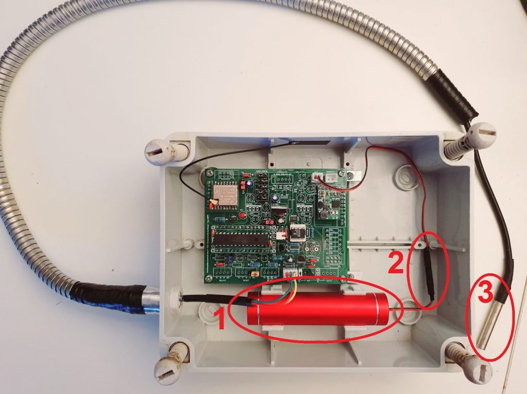
The following figure shows the housing of the electronic components inside the box.

Figure 2. Sensor box – internal components disposition

In the electrical box, in addition to the sensor control board described above, there is the backup battery (1). This is placed inside a cylindrical aluminum container anchored to the electrical box by PVC clips and is connected to the control board through a protection circuit to prevent excessive charge / discharge of the battery (2). The temperature sensor (3) is inserted inside a waterproof capsule and connected to the control board by an electric cable. The cable outside the box is protected by a steel coating tube. Here, a simple shower hose was used to protect the integrity of the cable from the external agents (rain, ice, snow, UV radiation, …).

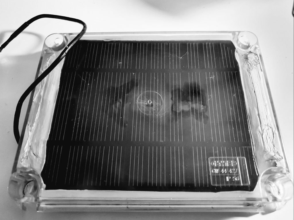
The battery is kept on charge by a photo-voltaic panel placed below the transparent lid of the box (figure 3).

Figura 3. Pannello solare per la ricarica della batteria

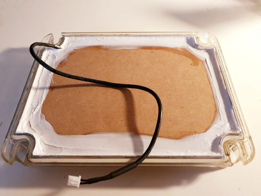
Inside the box, under the photo-voltaic panel, an MDF panel suitably shaped and sealed with silicone at the edges, creates a sort of interspace between the photo-voltaic panel and the lower part of the box hosting the electronics (figure 4).

Figure 4. Lower side of the box cover.

Not visible in the figure, the interspace has been filled with foam to obtain a thermal insulation between the lid and the lower part of the box to limit the temperature rise in summer time when the solar radiation is very intense.

In the final assembly, the sensor box is positioned on the roof next to the hot water tank. The capsule with the temperature sensor is inserted in a cockpit placed on one side of the tank (generally hot water tanks are equipped with a cockpit for analog temperature probes – in this case the analog probe can be removed and replaced with the digital probe).

Central unit

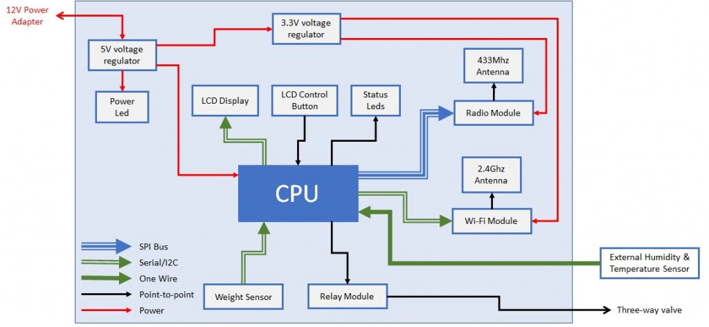
The central unit is the heart of the solution. Here follows the block diagram:

Central unit block diagram

The diagram includes:

  • Central processing unit (CPU)
  • 433Mhz radio transmission module and antenna
  • 2.4GHz WiFi connection module and antenna
  • 16×2 characters LCD Display module
  • Relay module used to control the flow switch valve
  • External humidity and temperatyre sensor
  • Weight sensoe
  • Multifunctional push button
  • Status/Power leds
  • 5v and 3.3v voltage regulators
  • 12v exernal power supply

The following figure shows the front panel of the control unit:

Figure 5. Central unit front panel

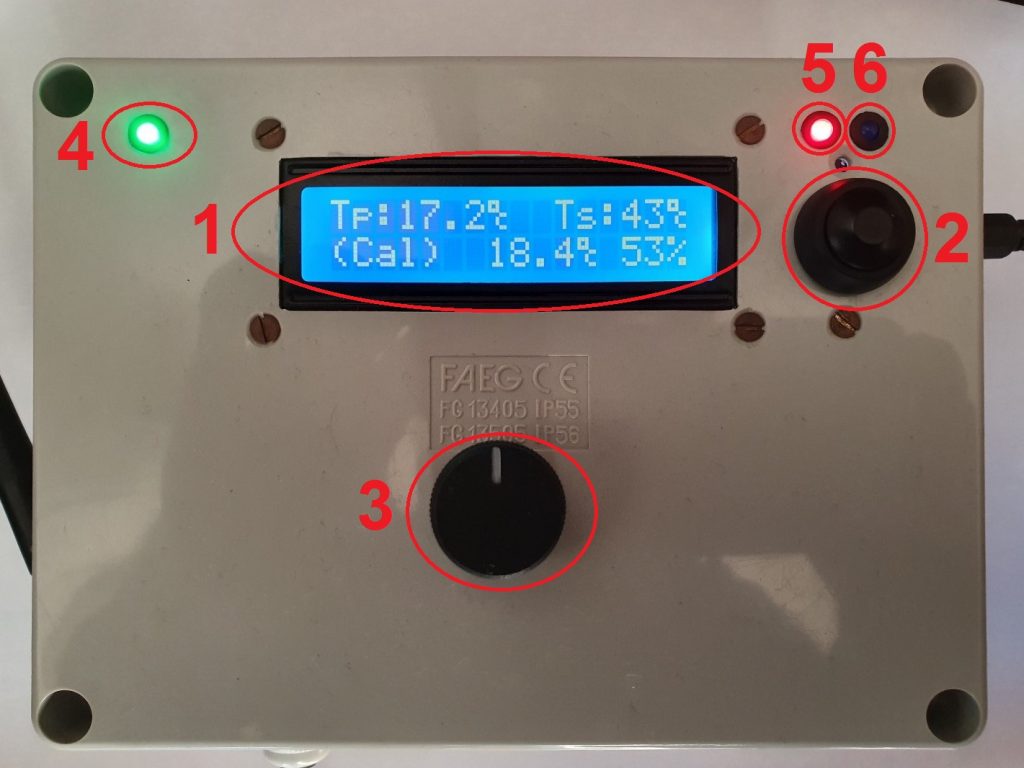
The electronic components are hosted inside a PVC electrical box. The front panel embeds the LCD display (1) for viewing working parameters and the operating status, the multifunctional button (2) is used to browse the different views of the display and operate the basic commands to configure and adjust the unit operating parameters, the knob used to regulate the exchange temperature (3), the indicator LEDs that allow you to quickly check the health status of the device: these are from left to right the power on indicator (4), the health of the radio link with the sensor (5), the status of the connection to the WiFi network (6). The following figures show the external sides of the unit.

Figure 6. External sides of the central unit: the left hand side, lower side and right hand side


On the left hand side there is the WiFi antenna (1), on the lower side there are the connection cable to the sensor for the ambient temperature and humidity (2) and the the auxiliary connector (3). This is used in this project by the weight sensor to measure the level of the condensate in the tank which is produced by the gas boiler. On the right hand side there are the 12V / 1A power supply connector (4) and the connector needed to drive the flow switch valve (5).

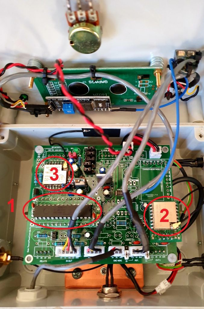
The main electronic board is placed inside the box (Figure 7) and includes the following components: (1) it is the CPU that is based on the Atmel ATmega328p microcontroller (ref. [1]), (2) it is the WiFi module for the connection to the internet that is based on the ESP8266 chip, (3) is the LoRa Ra-02 data transmission module (ref. [2]). The WiFi module model is the well-known ESP-07S produced by Ai-Thinker (ref. [3]) which is equipped with an external connector for the external WiFi antenna.

Figure 7. Inside the central unit box – main board

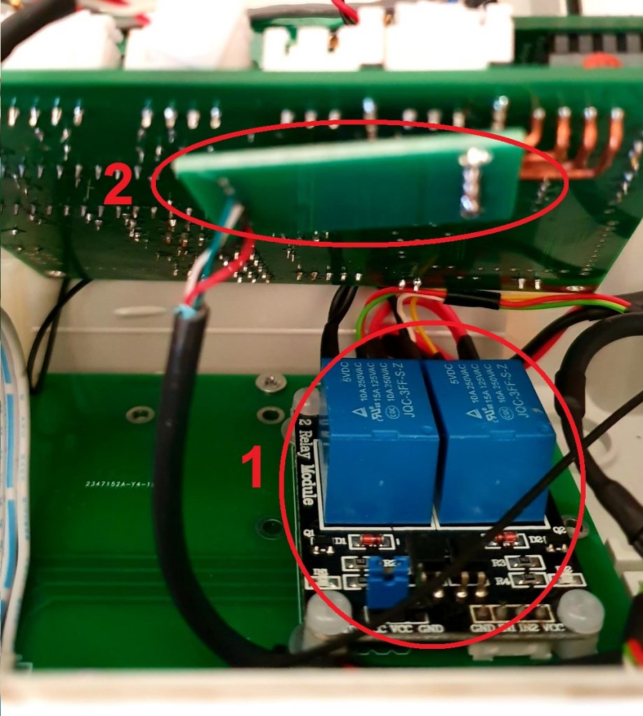
Under the main electronic board there is an auxiliary board (Figure 58) which hosts a pair of relays (1) required to drive the three-way flow exchange valve. In addition, the image reveals the HX711 module (2) located on the rear face of the main board. This module represents the interface with the sensor that measures the weight and therefore the level of condensate in the tank placed under the boiler.

Figure 8. Inside the central unit box – auxiliary board

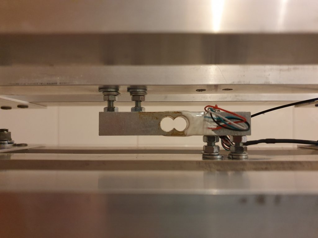
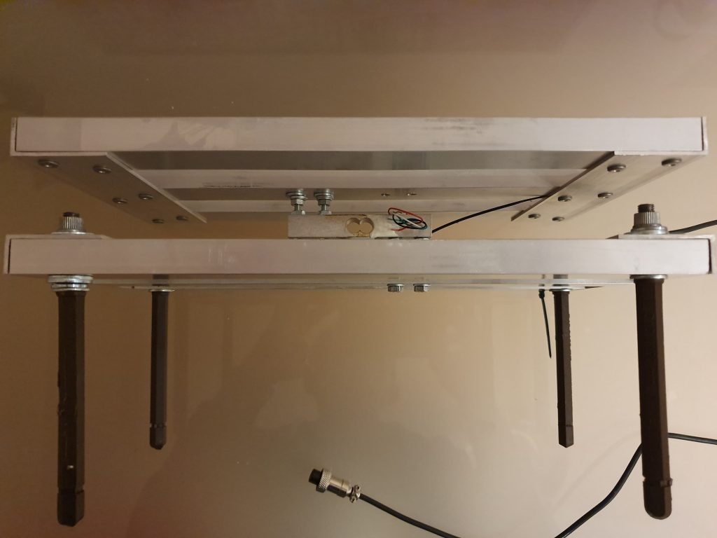
The tank for collecting the condensate rests on a weight scale made of two parallel plates interconnected by a torsion element (load cell) which represents the weight sensor (see ref. [5] for further details).

IoT and Monitoring

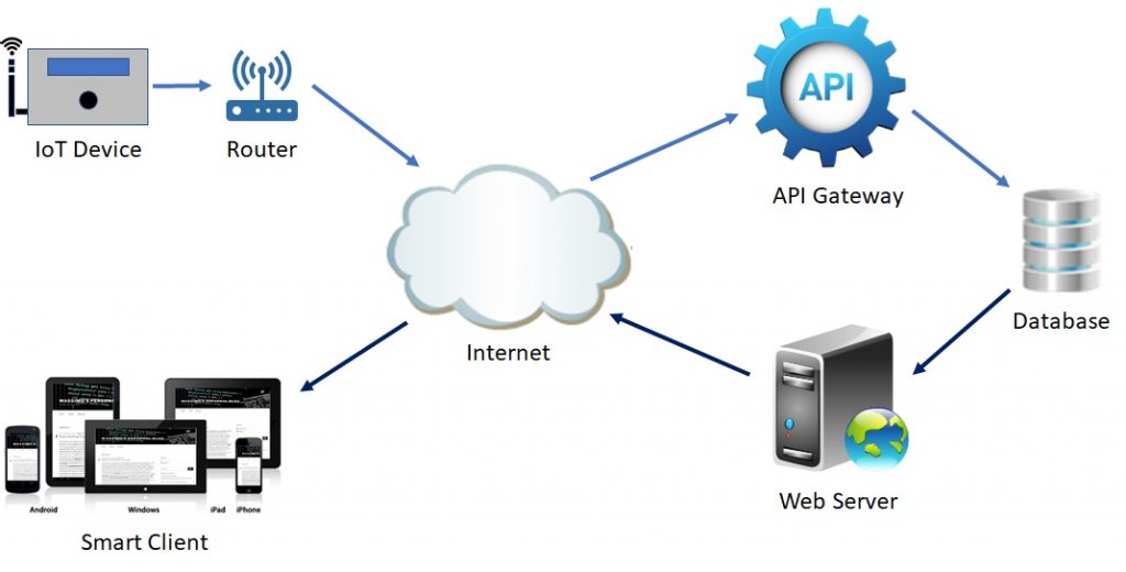
As mentioned above, the central unit has an ESP8266 module used to connect to home WiFi network. In this solution, the internet connection is used to send overall status information to an API service which saves it into a database. A web interface is then used to monitor the status of the controller from any device and location over the internet. Following picture shows the simple architecture of the API and monitoring service:

The API gateway exposes an API called directly from the central unit (IoT device) and stores status data to a MySQL database. The web server exposes a web page (php) that shows the latest status information using the graphical representation shown below:

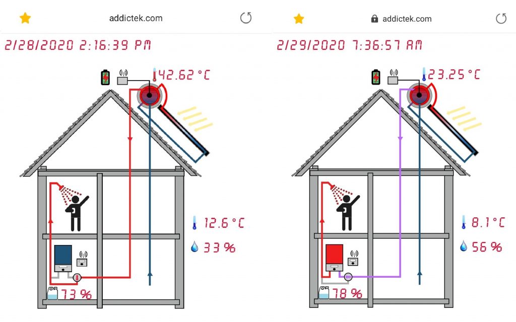
Two images of the monitoring page: on the left hand side picture, the tank water temperature is above the switching temperature (38 celsius degrees) and hence the gas boiler is bypassed; on the right side picture, the tank water temperature is below the switching temperature and hence the gas boiler heats up the water coming from the solar tank.

Status information shown in the picture includes:

  • Flow status
  • Solar tank water temperature
  • Sensor battery charging level and status
  • External temperature and humidity
  • Filling status of the tank for condensate placed below the gas boiler

In addition, the page can show various health monitoring alerts like:

  • The communication health status between the central unit and the sensor
  • The condensate tank level above 90%

References

[1] Atmel ATmega328p microcontroller – Microchip Technology

[2] Ai-Thinker LoRa Ra-02 radio transmission module

[3] Ai-Thinker ESP07-S WiFi Module

[4] MCP9700 linear thermistor for temperature measurement

[5] Article: Building an electronic weight scale using a load cell sensor

Low Power Current Sensor


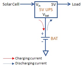
In this article we will see how realize a current sensor circuit in a device using Arduino or more in general the ATmega328P CPU. The current sensor will leverage the built-in ADC of ATmega328P and few external components. The current sensor will have a good level of accuracy and low power consumption, making the solution applicable even to battery powered devices. Specifically, I realized this solution to measure the charging and discharging current flowing to and from the backup battery used in the remote sensor which is part of the Solar Thermal Controller project (see ref. [1]). The backup battery is connected to an UPS module to provide continuos power to the the circuit. The UPS module receives input power from a solar cell and provides a 5v regulated power to the output. When the input power is above the load power the backup battery is kept under charge. Charging power is the difference between the available input power and the load power. When the input power is below the load power, the backup battery is used to source the missing power (see Figure 1).

Figure 1. UPS module and backup battery.

The battery charge/discharge current along with the battery voltage level are used to determine the state of charge (SoC) of the battery.

The technique used to measure the current is based on the Ohm’s law. A shunt resistor is connected in series to the battery between the anode and ground.
The current flowing into the battery and resistor are the same, the voltage drop on the shunt resistor is proportional to the intensity of the current.

\[
{V_{shunt} = I_{shunt} \cdot R_{shunt}}
\]

For the application scenario, I wanted to sense charging current up to 600mA and discharging current up to 150mA. With a 0.1Ω shunt resistor, this corresponds to a maximum voltage drop across the resistor of 0.06V while charging and -0.015V while discharging.

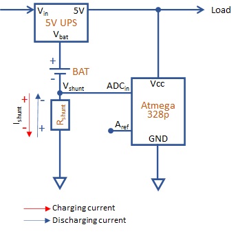
Wanting to sample this voltage drop directly with ATmega328P built-in ADC (see figure 2), we have two problems: 1) voltage drop is actually too low to be measured with acceptable accuracy. Even having a adequate voltage reference for the ADC, due to the low voltage range, the reading would possibly be affected by eccessive noise, 2) more important the voltage drop changes polarity, being positive during battery charge and negative during battery discharge .

Figure 2. ADC directly sampling the shunt resistor drop voltage

Here is where the use of an instrumentation operational amplifier comes in handy. An instrumentation amplifier is a kind of differential amplifier with additional input buffer stages to easily match the impedance of the amplifier with the preceding stage. Instrumentation amplifiers are commonly used in industrial test and measurement application and has some useful features like low offset voltage, high CMRR (Common mode rejection ratio), high input resistance and high gain.

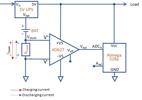
For the purpose of the application scenario described here, we need to select a model supporting single power supply and rail-to-rail output operation range. Second, we want it to sink very low current since we don’t want it to affect the measured current and reduce the battery backup time. There are several models that have similar capabilities, one of them is the AD627an by Analog Devices (see ref. [2]). The AD627an supports 85μA maximum supply current, single supply power starting from +2.2V and rail-to-rail output swing. As for other instrumentation amplifiers, the gain can be set with one external resistor. Figure 3 shows how the amplifier can be connected between the shunt resistor and ATmega328p for current sensing:

Figure 3. AD627 used to amplify shunt voltage drop before sampling it with the ADC

Note that the V negative input of the amplifier is connected to ground and V+ to the the other side of the shunt resistor. Having ground as reference, the voltage on V+ will be positive during battery charge (current flowing like the red arrow in the picture) and negative during battery discharge (current flowing like the blue arrow in the picture).

From the datasheet we see that the V+ amplifier input terminal can go from (−VS)−0.1V to (+VS)−1V, while the output can go from (−VS)+0.1V to (+VS)−0.15V. On the V+ input side, the ability of this amplifier to go 0.1V below the negative voltage supply (the ground in our case and hence V) is very important because we need to sense both positive and negative voltage drop accross the shunt resistor. Applying these specifications to the application scenario where −VS is 0V (GND) and +VS is 5V, will result in following absolute limits for V+ input voltage and Vout output voltage:

\[
-0.1V < V^+ < 4V
\]

\[
0.1V \lt V_{out} \lt 4.85V
\]

As stated above, the shunt resistor voltage drop will be from 0.015V to 0.06V which is well inside the supported range. Now we need to select appropriate values for the gain (G) and reference voltage Voff, the latter being the offset applied to amplifier output. Ideally, the input/output transfer function of the amplifier is:

\[
V_{out} = [(V^+)-(V^-)] \cdot G + V_{off}
\]

Hence, being V= 0:

\[
V_{out} = [(V^+)] \cdot G + V_{off}
\]

However, since the reality is different from theory, in order to stay within the amplifier operating limits, we need to refer to “INPUT RANGE LIMITATIONS IN SINGLE-SUPPLY APPLICATIONS” section of the datasheet and select proper gain and offset values.

The equation in the datasheet on page 16 is used to check the amplifier internal limits and is reported below:

\[
V_{A1} = 1.25 \cdot (V^- + 0.5V) – 0.25 \cdot V_{off}-\frac{(V^+ – V^-) \cdot 25k\Omega}{R_{G}}
\]

In the above equation, RG is the value of the external resistor used to set the amplifier gain and is calculated according to the following formula:

\[
G = 5 + \frac {200k\Omega}{R_{G}}
\]

\[
R_{G} = \frac {200k\Omega}{G – 5}
\]

The datasheet states that VA1 must be in the range from (−VS+50mV)=50mV to (+VS−200mV)=4.8V.

Setting a gain of 20 (RG=13.7 kΩ) and Voff = 1.235V, we have:

In case of V+=-0.015V:

\[
V_{A1}^{-} = 1.25 \cdot (0.5V) – 0.25 \cdot (1.235V) – \frac{ (-0.015V) \cdot 25k\Omega}{13.7k\Omega} = 0.343V
\]

In case of V+=0.06V:

\[
V_{A1}^{+} = 1.25 \cdot (0.5V) – 0.25 \cdot (1.235V) – \frac{ (0.06V) \cdot 25k\Omega}{13.7k\Omega} = 0.207V
\]

Both values are well within the admitted range.

On the output side, minimum and maximum values will be the following:

\begin{equation} \label{eq:voutmin}V_{out}^{-} = V_{ref} + (V^+ – V^-) \cdot R_{G} = 1.235V-0.015V \cdot 20 = 0.935V \end{equation}

\begin{equation} \label{eq:voutmax}V_{out}^{+} = V_{ref} + (V^+ – V^-) \cdot R_{G} = 1.235V+0.06V \cdot 20 = 2.435V \end{equation}

Again, both values are within the amplifier limits.

Sampling the amplifier output voltage with ATmega328P ADC, requires setting the proper voltage reference on the Aref pin. In this case, a +2.5V reference will allow the 10 bit ADC to sample the whole amplifier output range.

The current sensing precision depends on the ADC resolution and corresponds to the minimum change in current that the circuit will be able to sense. The ADC voltage resolution (ADCVres) is given by:

\[
ADC_{Vres} = \frac {A_{ref}}{2^N}
\]

Where N is the ADC resolution in bits which equals to 10 in case of ATmega328P. The variation of amplifier output voltage can be written as follows:

\[
\Delta V_{out} = \Delta (V^+ – V^-) \cdot G = \Delta V^+ \cdot G = R_{shunt} \cdot \Delta I_{shunt} \cdot G
\]

So,

\[
\Delta I_{shunt} = \frac{\Delta V_{out}}{R_{shunt} \cdot G}
\]

Substituting ΔVout with the ADC voltage resolution, we get the minimum variation Ishunt that can be sampled by the ADC, which is:

\begin{equation} \label{eq:1}
I_{res} = \frac {A_{ref}}{2^N \cdot R_{shunt} \cdot G} = \frac {2.5V}{1024 \cdot 0.1\Omega \cdot 20} = 1.23mA/unit
\end{equation}

The formula to calculate the current flowing on the shunt resistor is the following:

\begin{equation} \label{eq:2}
V_{out}=V^+ \cdot G + V_{off} = I_{shunt} \cdot R_{shunt} \cdot G + V_{off}
\end{equation}

The value sampled by the ADC depends on the ADC input voltage (Vout), the voltage reference value (Aref) and the ADC bit resolution (N) and can be written as follows:

\begin{equation} \label{eq:3}
ADC = \frac {V_{out} \cdot 2^N}{A_{ref}}
\end{equation}

Getting Vout off (\ref{eq:3}) and substituting in (\ref{eq:2}) results in:

\begin{equation} \label{eq:4}
\frac {ADC \cdot A_{ref}}{2^N} = I_{shunt} \cdot R_{shunt} \cdot G + V_{off}
\end{equation}

Finally, we can get Ishunt off (\ref{eq:3}):

\begin{equation} \label{eq:5}
I_{shunt} = \frac{\frac {ADC \cdot A_{ref}}{2^N}-V_{off}}{R_{shunt} \cdot G}
\end{equation}

Equation (\ref{eq:5}) can be used in the sample algorithm to calculate the shunt current from the ADC sample value. Ishunt will be negative if battery is discharging and positive if battery is charging.

Sampling accuracy considerations

There are some principles that is worth taking into account to improve sampling accuracy. Their application is general and not strictly related to the use case described in this article.

Adjusting the voltage offset

You might have noticed in the above description that the sampling interval of the ADC is not fully used. This is because the offset value of the amplifier is almost centered within the ADC sampling interval (1.235V vs. [0V-2.5V]). This is good if the extension of the negative input range of the amplifier is the same as the positive input range. However, in our case, negative range is [-0.015V, 0V] and positive range [0V, +0.06V]. With a centered offset, the amplifier output will never go below 0.935V and above 2.435V (see (\ref{eq:voutmin}) and (\ref{eq:voutmax})) while the ADC will still be able to sample the whole range from 0V to Aref=2.5V. In other words, we are wasting part of the sample interval which means reducing the practical ADC voltage resolution. Figure 4 shows the amplifier input range vs output range in case of (a) centered voltage offset value (b) adjusted voltage offset value:

Figure 4. Amplifier input range vs output range in case of (a) centered voltage offset value (b) adjusted voltage offset value

Let’s see how to calculate the appropriate voltage offset for the amplifier according to the negative and positive extension of the input range, ADC reference voltage Aref and shunt resistor value Rshunt :

Figure 5. Amplifier input vs. output range

Being the amplifier input voltage going from -0.015V to 0.06V the correct voltage offset can be calculated solving the following equality (see Figure 5):

\[
(V_{off}-V_{out}^{min}):(V_{out}^{max}-V_{out}^{min}) = (V^+_0-V^+_{min}):(V^+_{max}-V^+_{min})
\]

\[
V_{off} = \frac {(V_{out}^{max}-V_{out}^{min}) \cdot (V^+_0-V^+_{min})}{(V^+_{max}-V^+_{min})} + V_{out}^{min}
\]

Since amplifier output range must match the ADC sample the interval that is [Voutmin, Voutmax] = [0, Aref], we get:

\[
V_{off} = \frac {A_{ref} \cdot (V^+_0-V^+_{min})}{(V^+_{max}-V^+_{min})}
\]

Substituting actual values:

\[
V_{off} = \frac {A_{ref} \cdot 0.015V}{0.075V} = 0.5V
\]

Setting the amplifier offset to +0.5V would allow us to increase the gain:

\[
G = \frac {V_{out}^{max}-V_{out}^{min}}{V^+_{max}-V^+_{min}} = \frac {A_{ref}}{V^+_{max}-V^+_{min}} = \frac {2.5V}{0.075V} = 33
\]

Setting the new gain value in equation (\ref{eq:1}), will give us the updated sampling precision :

\[
I_{res} = \frac {A_{ref}}{2^N \cdot R_{shunt} \cdot G} = \frac {2.5V}{1024 \cdot 0.1\Omega \cdot 33} = 0.75mA/unit
\]

Averaging and Oversampling

Signal averaging and oversamplig are common techniques used to increase current sampling accuracy. In order to make these techniques effective we need to make some assumptions:

  • Sampled variable is the sum of two components: signal and noise
  • Signal s and noise z are uncorrelated
  • Signal measurements s(t) over sampling interval ΔT are strongly correlated, ideally signal power is constant
  • Noise measurements z(t) are random (uncorrelated) over sampling interval ΔT, the mean is 0 and the variance is constant.

Under these assumptions the Signal To Noise Ratio (SNR) can be calculated as follows:

\[
SNR = \frac{P_{signal}}{P_{noise}} = \frac {E[s^2]}{E[z^2]} = \frac {E[s^2]}{\sigma_z^2}
\]

Averaging

Averaging consists in sampling a random variable mutiple times and then calculating the average value of the samples. Let’s suppose we are sampling a random variable at dt time interval. The random variable is the sum of the signal s and random noise z. Averaging by a factor n consists in sampling the the value of the random variable n times in the dt time interval (the sample is taken every dt/n) and then averaging the n values. Another possibility is to keep the sampling interval at dt and implementing a moving average filter. The value of the sample is calculated every time the value is sampled by averaging on the last n values. The first teqnique implies increasing the sample frequency on n factor which is basically oversampling. Oversampling can also be used to increase the ADC resolution as decribed below.

Let’s go back to the noise component of our samples and assume that we just sample the noise. Let’s consider n consecutive samples of the noise, Z={z1, z2, …, zn}, having per-sample variance of σ2z. It can be demostrated that (see [3]):

\[
E(\overline{z}^2) = Var(E[Z]) = Var({ \frac {1}{n} \sum_{i=1}^{n} z_i}) = \frac {1}{n} \sigma ^2_z
\]

The variance of the average of n samples is reduced by a factor of n thus improving the SNR by the same factor:

\[
\overline {SNR} = \frac{P_{signal}}{P_{noise}} = \frac {E[s^2]}{E(\overline{z}^2)} = n \frac {E[s^2]}{\sigma_z^2} = n \cdot SNR
\]

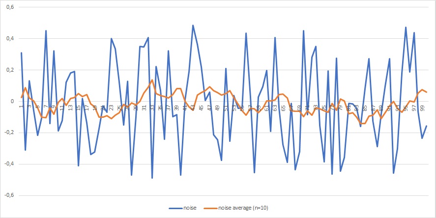
Following picture shows how visible is the benefit in noise reduction averaging a random variable by a factor of 10:

Figure 6. Noise distribution. Plain noise vs noise averaged on 10 samples
Oversampling

Oversampling consists in sampling the ADC input signal by a frequency that is higher than the required sampling rate fs. In accordance with the Nyquist Theorem, this is usually the Nyquist frequency fn corresponding to, the double of highest frequency component fm of interest in the input signal.

\[
f_s \gt f_n = 2 \cdot f_m
\]

For each additional bit of resolution (see ref. [4] and [5]), the signal must be oversampled by a factor of four, in general the oversampling frequecy fos is given by:

\[
f_{os} = 4^w \cdot f_s
\]

Where w is the number of additional bits of resolution desired.

For example to increase the resolution of the ATmega328P ADC of 2 additional bits (from 10 to 12 bits) we need to oversample by a factor of 16 (42). We need to cumulate 16 consecutive readings and then average the result by 4 (or right shift the sum by 2 bits). This is also referred as decimation process. This way we will have a 12 bit effective sample with an improvement in the SNR (Signal to Noise Ratio).

Circuit design considerations

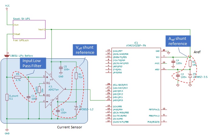
Following pictures shows the final circuit schema for the current sensor:

Figure 7. Current sensor circuit schematic

The circuit implements the current sensor design described in previous paragraphs. There are few additional modules required by the circuit whose components need correct sizing:

  • Instrumental amplifier input low pass filter
  • Voff and Vref voltage shunt regulators

Amplifier input low pass filter

An input low pass filter to the instrumentation amplifier is highly recommended to filter out RF interference. In fact, instrumentation amplifiers can rectify high frequency out of-band signals. Once rectified, these signals appear as dc offset errors at the output. RF interference can be present for example in circuits making use of buck-boost converters that usually operate at frequencies beetween 600Khz and 1.5Mhz. For example the UPS module used in this circuit is using a boost converter to generate a regulated 5V output from the battery voltage.

To suppress these RF interferences, a low pass RC filter can be added to the amplifier input. Resistor R3 and capacitor C1 provide such filter, with a cut off frequency (-3db frequency corresponding to 50% signal power reduction):

\[
f_c = \frac {1}{2 \pi \cdot (R3 \cdot C1)} = \frac {1}{2 \pi \cdot (4,7k\Omega \cdot 100nF)} = 338Hz
\]

R3 and C1 provide a 338Hz cut off frequency that is enough for the purpose of the current sensor, assuming that the measured signal (shunt voltage drop) is quite stable over time.

Voltage shunt regulators

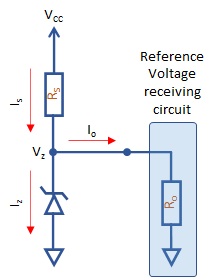
Shunt regulators diodes are used in the circuit to provide a precise and stable voltage reference to the instrumentation amplifier (offset voltage) and the ADC (reference voltage). Diodes used here belong to LM285/385-xxx series from Texas Instruments (see ref. [6]). The LM285/385-xxx are micropower 3-terminal current band-gap voltage reference diodes. They are designed to operate over a wide current range as low as 10µA up to 20mA, with low noise and stable operation over time and temperature. In particular, we selected the LM385z-1.2 for the amplifier offset voltage (Voff) and LN385z-2.5 for the ADC reference voltage (Aref). The regulator circuit is very simple and only requires some precautions in sizing the series resistor to provide the current required by the diode to operate correctly. One important thing to consider is the input impedance of the circuit receiving the refrerence voltage. Following picture shows the typical application circuit:

Figure 8. Shunt voltage regulator application circuit

Where:

  • Vcc is the unregulated input voltage
  • Vz is the shunt regulator (zener) voltage
  • Rs is the current limiting resistor
  • Ro is the input impedance of the receiving circuit

Iz must be greater than the maximum value of the minimum operating current (Izmin) required by the reference diode. In case of LM385z-xxx the maximum value of the minimum operating current is between 20µA and 30µA over the whole operating temperature range depending on the regulator voltage (see ref. [6]):

\begin{equation} \label{eq:Iz}
I_z = I_s – I_o \gt I_z^{min}
\end{equation}

Where:

\begin{equation} \label{eq:Is}
I_s = \frac{V_{cc} – V_z}{R_s}
\end{equation}

\begin{equation} \label{eq:Io}
I_o = \frac{V_z}{R_o}
\end{equation}

Hence, substituting (\ref{eq:Is}) and (\ref{eq:Io}) in (\ref{eq:Iz}):

\[
I_z = \frac{V_{cc} – V_z}{R_s} – \frac{V_z}{R_o} \gt I_z^{min}
\]

Finally, the constraint on Rs is the following:

\begin{equation} \label{eq:Rs}
R_s \lt \frac {R_o \cdot (V_{cc} – V_z)}{R_o \cdot I_z^{min} + V_z} = \frac {V_{cc} – V_z}{ I_z^{min} + \frac {V_z}{R_o}}
\end{equation}

To reduce power consumption we want to determine the maximum possible value for Rs that results from (\ref{eq:Rs}) replacing the maximum value of the Iz current and the minimum value of Ro resistance. These values can be read from components datasheets.

Amplifier offset shunt regulator

For the shunt regulator connected to the Voff pin of the instrumentation amplifier we have:

Minimum input impedance for AD627 Voff pin (see ref. [2] “AD627 Reference Input Impedance” on Table 3, pag 6) is:

\[
R_o \gt 125k\Omega
\]

Maximum value of the minimum operating current for the shunt diode (see ref. [6] “Minimum Operating Current” max value for LM385-1.2) is:

\[
I_z^{min} \lt 20 \mu A
\]

Substituting above values in (\ref{eq:Rs}):

\[
R_s \lt 126k\Omega
\]

ADC reference shunt regulator

For the shunt regulator connected to the Aref pin of the ATmega328P we have:

Minimum input impedance for ATmega328P Aref pin (see ref. [7] “Reference input resistance” on Table 28-8):

\[
R_o \gt 22.4k\Omega
\]

Maximum value of the minimum operating current for the shunt diode (see ref. [6] “Minimum Operating Current” max value for LM385-2.5) is:

\[
I_z^{min} \lt 30 \mu A
\]

Substituting above values in (\ref{eq:Rs}):

\[
R_s \lt 18k\Omega
\]

References

[1] Massimo Morlupi. Solar Heating Controller. , 2020.
[Bibtex]
@article{solarheatingcontroller,
author = "Massimo Morlupi",
title = "{Solar Heating Controller}",
year = "2020"
}
[2] Analog Devices. Micropower, Single- and Dual-Supply, Rail-to-Rail Instrumentation Amplifier. , 2013.
[Bibtex]
@ad627{ad627,
author = "Analog Devices",
title = "{Micropower, Single- and Dual-Supply, Rail-to-Rail Instrumentation Amplifier}",
year = "2013"
}
[3] Howard E. Haber. Class Handouts – iid random variables. , 2012.
[Bibtex]
@iid{iid,
author = "Howard E. Haber",
title = "{Class Handouts - iid random variables}",
year = "2012"
}
[4] Silicon Labs. Improving ADC Resolution by Oversampling and Averaging. , rev 1.3.
[Bibtex]
@an118{an118,
author = "Silicon Labs",
title = "{Improving ADC Resolution by Oversampling and Averaging}",
year = "rev 1.3"
}
[5] Atmel. AVR121: Enhancing ADC resolution by oversampling. , 2005.
[Bibtex]
@avr121{avr121,
author = "Atmel",
title = "{AVR121: Enhancing ADC resolution by oversampling}",
year = "2005"
}
[6] ON Semiconductor. LM285/LM385 Micropower Voltage References. , 2016.
[Bibtex]
@lmx85{lmx85,
author = "ON Semiconductor",
title = "{LM285/LM385 Micropower Voltage References}",
year = "2016"
}
[7] Atmel Corporation. ATmega328P – 8-bit AVR Microcontroller with 32K Bytes In-System Programmable Flash. , 2015.
[Bibtex]
@atmega328p{atmega328p,
author = "Atmel Corporation",
title = "{ATmega328P - 8-bit AVR Microcontroller with 32K Bytes In-System Programmable Flash}",
year = "2015"
}

Building an electronic weight scale using a load cell sensor

Abstract

Load cells leverage the property of some materials that change their electrical resistance when subjected to compression and traction which determine their elastic deformation. The most common load cells available on the market have the shape of a metal bar with holes drilled in the central part to facilitate deformation (Figure 1).

Figure 1. Load Cell

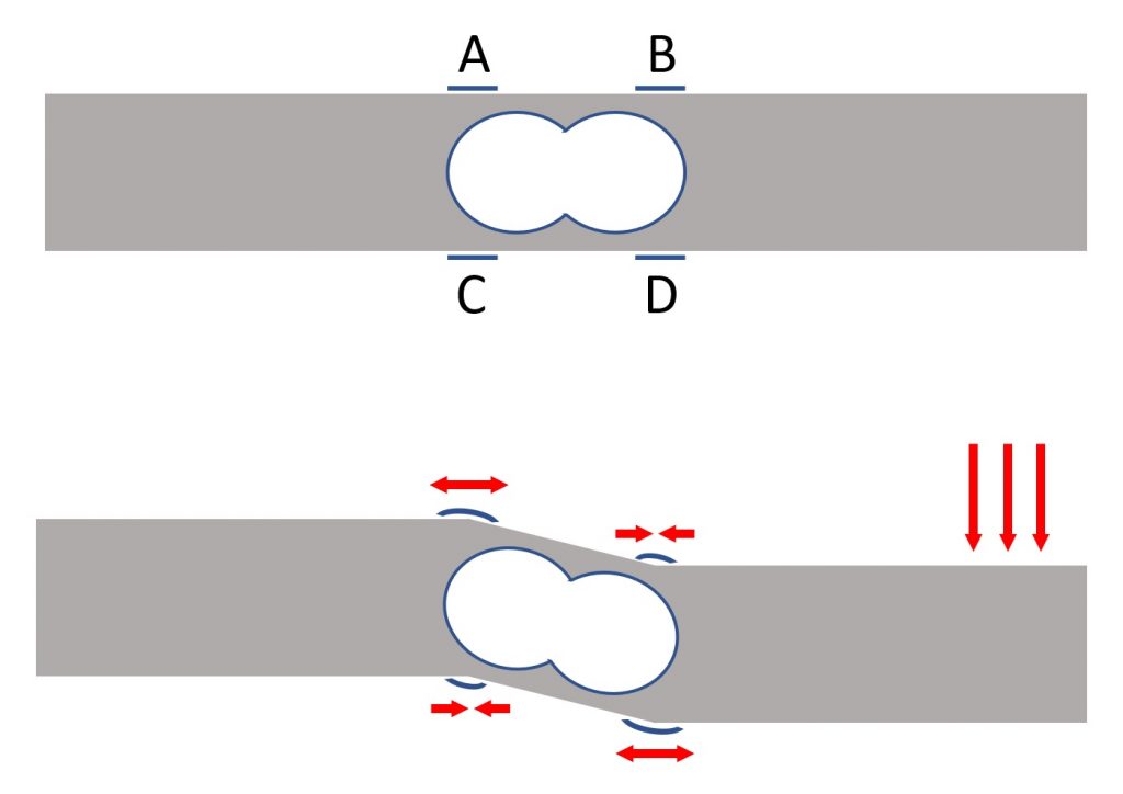
In their typical use, the cells are blocked at one end and the weight applied to the opposite end. Strain gauges are inserted in the center of the bar, on the upper and lower faces with respect to the holes, which can be assimilated to resistive elements that change their electrical characteristics according to the level of deformation (extension or compression) to which they are subjected (Figure 2).

Figure 2. Load cell at rest and on load

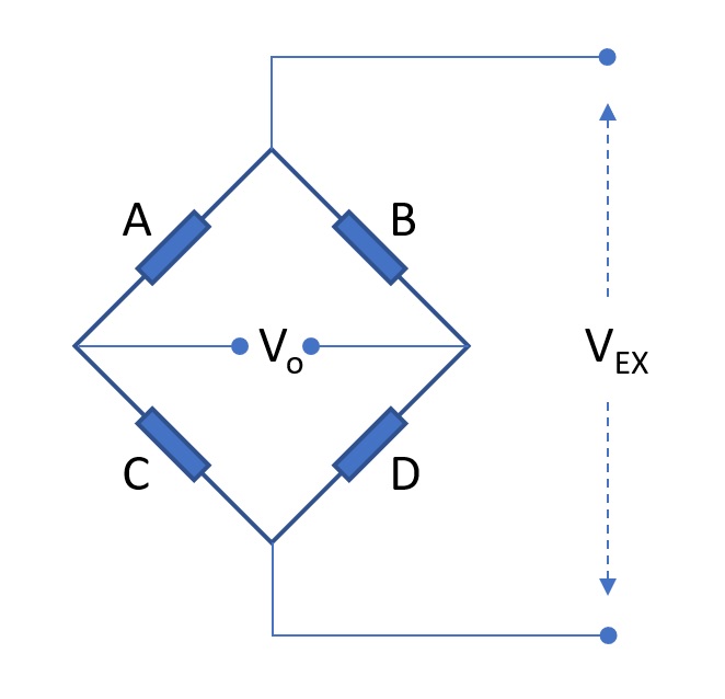
These elements are linked together to form a Wheatstone bridge (Figure 3). The bridge is excited with an input voltage (Vex), and is able to generate an electrical output signal (Vo) proportional to the imbalance of resistive value between the elements A-C and B-D. At rest all the elements have the same resistive value, the bridge is balanced and the output voltage is zero. Under load the values ​​of the resistances change and consequently the value of the output voltage is proportional to the applied load.

Figure 3. Wheatstone bridge

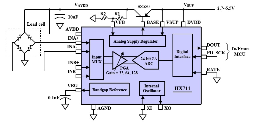
To adequately sample the electrical output signal, the integrated circuit already set up for this type of application can be used. This is the HX711 (ref. [1]) whose block diagram is shown below:

Figure 4. HX711 internal block diagram

The electrical output signal of the load cell (Wheatstone bridge) is sent to one of the two input channels of the HX711 (channel selection is made through a multiplexer located at the input). Subsequently it is amplified by an operational amplifier with adjustable gain (32, 64 or 128) and finally sampled by a 24bit analog-digital converter (ADC). To read the sampled value, the HX711 provides a serial interface controlled by a clock signal. On the rising edges of the clock signal (PD_SCK) the 24 bits of the sampled value are made available on pin D_OUT one after the other. There are several libraries for Arduino and other microcontrollers for interfacing with this component.

The balance

The basic elements of the balance are the plates. Both plates are made of aluminum bars tightened at the ends by angular profiles:

Figure 5. Building elements of the balance

The aluminum elements are held together by steel rivets. The lower plate is used as a support base for the balance while the upper plate is used to support the load to be measured. The load cell is inserted in a “sandwitch” between two plates and anchored to the central bars of the lower plate at one end and the upper plate at the other end:

Figure 6. Anchoring of the load cell to the weighing plates

The following figure shows the balance in its final assembly:

References

[1] HX711 datasheet

DSA: cosa sono e strumenti di supporto

Tachistoscopio

Si tratta di uno strumento per strutturare e migliorare la capacità, la velocità e la correttezza della lettura. E’ utilizzabile in presenza di dislessia o di altri disturbi che coinvolgono e complicano la capacità di leggere. E’ generalmente impiegato in ambito logopedico nei percorsi riabilitativi per esercitare  e potenziare la capacità di leggere.

Il tachistoscopio espone chi lo usa a stimoli visivi di durata breve e variabile: nel caso dei disturbi che coinvolgono la lettura, si usa per proporre esercizi di visualizzazione di liste di parole, per migliorare il riconoscimento visivo e la lettura veloce e globale della parola come unità, a “colpo d’occhio”, senza ricorrere alla lettura fonologica che procede lettera per lettera.

Lo strumento può essere utilizzato durante le sessioni di logopedia in presenza di uno specialista ma anche in modo autonomo a casa o altro luogo per continuare ad esercitare le proprie capacità di lettura.

Generalmente gli specialisti sono dotati di programmi software che includono questi strumenti tuttavia il loro utilizzo da parte del paziente può richiedere l’acquisto di una licenza software il cui costo può essere significativo. Per questa ragione, ho deciso di sviluppare alcuni di questi strumenti e metterli a disposizione degli utilizzatori (specialisti o pazienti) a titolo gratuito. Di seguito il link al tachistoscopio:

Tachistoscopio

Le istruzioni per utilizzarlo sono molto semplici. La schermata principale presenta una finestra di dialogo in alto a sinistra con i parametri di funzionamento:

  • Intervallo: è l’intervallo di tempo che intercorre tra la visualizzazione di una parola e la successiva. E’ espresso in millesimi di secondo, il valore di base è 2000 corrispondente a 2 secondi.
  • Tempo di esposizione: è il tempo di visualizzazione della singola parola sempre in millesimi di secondo, il valore di base è 500 corrispondente a mezzo secondo.
  • Posizione: è la posizione nella pagina all’interno della quale viene visualizzata la parola. Ci sono 9 posizioni selezionabili su una griglia di suddivisione della pagina di 3×3 caselle.
  • Lista: è la lista di parole da utilizzare. Ci sono alcune liste preimpostate utilizzabili per verificare il funzionamento dello strumento e dei diversi parametri di configurazione. E’ possibile visualizzare l’elenco delle parole della lista selezionata utilizzando il pulsante “Anteprima” e caricare una propria lista utilizzando il pulsante “Carica”. La lista è un semplice file di testo contenente una parola per riga. Una volta caricata la propria lista sarà possibile selezionarla dal menu a tendina. Il nome della lista corrisponderà con quello del file di testo utilizzato per il caricamento. Si noti che non è necessario inserire le parole divise in sillabe, così come non è necessario rispettare una regola sulle minuscole e maiuscole. Lo strumento gestisce questi aspetti in autonomia secondo le impostazioni che seguono.
  • Attiva sillabazione: se questa opzione è attivata, le parole saranno automaticamente suddivise in sillabe dallo strumento. La spaziatura fra una sillaba e la successiva potrà essere specificata con l’opzione seguente.
  • Spazi fra le sillabe: se l’opzione precedente è attiva, questo valore corrisponde al numero di spazi tra una sillaba e la successiva.
  • Verifica la parola: se questa opzione è attiva, dopo la visualizzazione di una parola verrà mostrato un dialogo di input nel quale l’utente dovrà inserire la parola appena vista. In caso di errore, lo strumento lo segnala in modo chiaro cambiando il colore del dialogo in rosso per un breve istante. Nel caso non fosse possibile inserire la parola corretta si potrà saltare il controllo inserendo la parola vuota. In tal senso questa opzione può anche essere utilizzata per regolare manualmente l’intervallo fra una parola e la successiva.
  • Ordine casuale: se attivata questa opzione consente di esporre le parole della lista in ordine casuale.
  • Dimensione carattere: è la dimensione del font utilizzata per visualizzare le parole.
  • Stile parola: è lo stile maiuscolo/minuscolo utilizzato per visualizzare le parole.

Una volta impostati i parametri desiderati, si può iniziare l’esercitazione premendo il pulsante “Inizia“. In qualsiasi momento è possibile interrompere l’esercitazione premendo il tasto “Esc” della tastiera. E’ consigliabile utilizzare sempre questo metodo per interrompere e riprendere una esercitazione perché viene mantenuta l’impostazione dei parametri, comprese eventuali liste caricate manualmente. Ricaricando la pagina del browser si perderebbero invece tutte le impostazioni fatte.

Cronotesto

Una variante del tachistoscopio è il “cronotesto”. Si tratta di un visualizzatore di testi che permette di esercitarsi nella lettura di un flusso di parole organizzate in un testo, secondo velocità e modalità di visualizzazione specifiche. Il testo viene visualizzato parola per parola secondo il verso naturale di lettura. E’ possibile impostare i seguenti parametri:

  • Intervallo fra le parole: è l’intervallo di tempo in millisecondi che intercorre fra la visualizzazione di una parola e la successiva.
  • Sillabe al secondo: il tempo di permanenza di una parola (in secondi) è dato dal numero di sillabe moltiplicato per questo parametro. Ad esempio se il numero di sillabe al secondo è 3, una parola di tre sillabe rimarrà attiva per 1 secondo, una parola di 6 sillabe per 2 secondi, una parola monosillabica per 1/3 di secondo.
  • Testo: è il testo da utilizzare nell’esercitazione. Ci sono alcuni testi preimpostati utilizzabili per verificare il funzionamento dello strumento e dei diversi parametri di configurazione. E’ possibile visualizzare il contenuto del testo utilizzando il pulsante “Anteprima” e caricare un proprio testo utilizzando il pulsante “Carica”. Il file contenente il testo deve essere di tipo testo (.txt) non è possibile utilizzare i formati pdf o word. Una volta caricato, il testo sarà reso disponibile nel menu a tendina. Il nome del testo corrisponderà con quello del file di testo utilizzato per il caricamento.
  • Dimensione carattere: è la dimensione del font utilizzata per visualizzare le parole.

Di seguito il link allo strumento: Cronotesto