In this article we will see how realize a current sensor circuit in a device using Arduino or more in general the ATmega328P CPU. The current sensor will leverage the built-in ADC of ATmega328P and few external components. The current sensor will have a good level of accuracy and low power consumption, making the solution applicable even to battery powered devices. Specifically, I realized this solution to measure the charging and discharging current flowing to and from the backup battery used in the remote sensor which is part of the Solar Thermal Controller project (see ref. [1]). The backup battery is connected to an UPS module to provide continuos power to the the circuit. The UPS module receives input power from a solar cell and provides a 5v regulated power to the output. When the input power is above the load power the backup battery is kept under charge. Charging power is the difference between the available input power and the load power. When the input power is below the load power, the backup battery is used to source the missing power (see Figure 1).
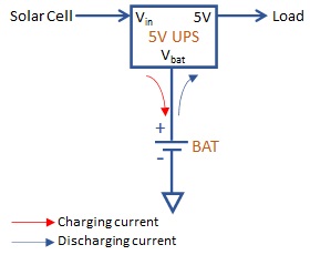
The battery charge/discharge current along with the battery voltage level are used to determine the state of charge (SoC) of the battery.
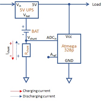
The technique used to measure the current is based on the Ohm’s law. A shunt resistor is connected in series to the battery between the anode and ground.
The current flowing into the battery and resistor are the same, the voltage drop on the shunt resistor is proportional to the intensity of the current.
\[
{V_{shunt} = I_{shunt} \cdot R_{shunt}}
\]
For the application scenario, I wanted to sense charging current up to 600mA and discharging current up to 150mA. With a 0.1Ω shunt resistor, this corresponds to a maximum voltage drop across the resistor of 0.06V while charging and -0.015V while discharging.
Wanting to sample this voltage drop directly with ATmega328P built-in ADC (see figure 2), we have two problems: 1) voltage drop is actually too low to be measured with acceptable accuracy. Even having a adequate voltage reference for the ADC, due to the low voltage range, the reading would possibly be affected by eccessive noise, 2) more important the voltage drop changes polarity, being positive during battery charge and negative during battery discharge .
Here is where the use of an instrumentation operational amplifier comes in handy. An instrumentation amplifier is a kind of differential amplifier with additional input buffer stages to easily match the impedance of the amplifier with the preceding stage. Instrumentation amplifiers are commonly used in industrial test and measurement application and has some useful features like low offset voltage, high CMRR (Common mode rejection ratio), high input resistance and high gain.
For the purpose of the application scenario described here, we need to select a model supporting single power supply and rail-to-rail output operation range. Second, we want it to sink very low current since we don’t want it to affect the measured current and reduce the battery backup time. There are several models that have similar capabilities, one of them is the AD627an by Analog Devices (see ref. [2]). The AD627an supports 85μA maximum supply current, single supply power starting from +2.2V and rail-to-rail output swing. As for other instrumentation amplifiers, the gain can be set with one external resistor. Figure 3 shows how the amplifier can be connected between the shunt resistor and ATmega328p for current sensing:
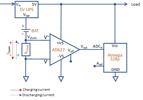
Note that the V– negative input of the amplifier is connected to ground and V+ to the the other side of the shunt resistor. Having ground as reference, the voltage on V+ will be positive during battery charge (current flowing like the red arrow in the picture) and negative during battery discharge (current flowing like the blue arrow in the picture).
From the datasheet we see that the V+ amplifier input terminal can go from (−VS)−0.1V to (+VS)−1V, while the output can go from (−VS)+0.1V to (+VS)−0.15V. On the V+ input side, the ability of this amplifier to go 0.1V below the negative voltage supply (the ground in our case and hence V–) is very important because we need to sense both positive and negative voltage drop accross the shunt resistor. Applying these specifications to the application scenario where −VS is 0V (GND) and +VS is 5V, will result in following absolute limits for V+ input voltage and Vout output voltage:
\[
-0.1V < V^+ < 4V
\]
\[
0.1V \lt V_{out} \lt 4.85V
\]
As stated above, the shunt resistor voltage drop will be from −0.015V to 0.06V which is well inside the supported range. Now we need to select appropriate values for the gain (G) and reference voltage Voff, the latter being the offset applied to amplifier output. Ideally, the input/output transfer function of the amplifier is:
\[
V_{out} = [(V^+)-(V^-)] \cdot G + V_{off}
\]
Hence, being V– = 0:
\[
V_{out} = [(V^+)] \cdot G + V_{off}
\]
However, since the reality is different from theory, in order to stay within the amplifier operating limits, we need to refer to “INPUT RANGE LIMITATIONS IN SINGLE-SUPPLY APPLICATIONS” section of the datasheet and select proper gain and offset values.
The equation in the datasheet on page 16 is used to check the amplifier internal limits and is reported below:
\[
V_{A1} = 1.25 \cdot (V^- + 0.5V) – 0.25 \cdot V_{off}-\frac{(V^+ – V^-) \cdot 25k\Omega}{R_{G}}
\]
In the above equation, RG is the value of the external resistor used to set the amplifier gain and is calculated according to the following formula:
\[
G = 5 + \frac {200k\Omega}{R_{G}}
\]
\[
R_{G} = \frac {200k\Omega}{G – 5}
\]
The datasheet states that VA1 must be in the range from (−VS+50mV)=50mV to (+VS−200mV)=4.8V.
Setting a gain of 20 (RG=13.7 kΩ) and Voff = 1.235V, we have:
In case of V+=-0.015V:
\[
V_{A1}^{-} = 1.25 \cdot (0.5V) – 0.25 \cdot (1.235V) – \frac{ (-0.015V) \cdot 25k\Omega}{13.7k\Omega} = 0.343V
\]
In case of V+=0.06V:
\[
V_{A1}^{+} = 1.25 \cdot (0.5V) – 0.25 \cdot (1.235V) – \frac{ (0.06V) \cdot 25k\Omega}{13.7k\Omega} = 0.207V
\]
Both values are well within the admitted range.
On the output side, minimum and maximum values will be the following:
\begin{equation} \label{eq:voutmin}V_{out}^{-} = V_{ref} + (V^+ – V^-) \cdot R_{G} = 1.235V-0.015V \cdot 20 = 0.935V \end{equation}
\begin{equation} \label{eq:voutmax}V_{out}^{+} = V_{ref} + (V^+ – V^-) \cdot R_{G} = 1.235V+0.06V \cdot 20 = 2.435V \end{equation}
Again, both values are within the amplifier limits.
Sampling the amplifier output voltage with ATmega328P ADC, requires setting the proper voltage reference on the Aref pin. In this case, a +2.5V reference will allow the 10 bit ADC to sample the whole amplifier output range.
The current sensing precision depends on the ADC resolution and corresponds to the minimum change in current that the circuit will be able to sense. The ADC voltage resolution (ADCVres) is given by:
\[
ADC_{Vres} = \frac {A_{ref}}{2^N}
\]
Where N is the ADC resolution in bits which equals to 10 in case of ATmega328P. The variation of amplifier output voltage can be written as follows:
\[
\Delta V_{out} = \Delta (V^+ – V^-) \cdot G = \Delta V^+ \cdot G = R_{shunt} \cdot \Delta I_{shunt} \cdot G
\]
So,
\[
\Delta I_{shunt} = \frac{\Delta V_{out}}{R_{shunt} \cdot G}
\]
Substituting ΔVout with the ADC voltage resolution, we get the minimum variation Ishunt that can be sampled by the ADC, which is:
\begin{equation} \label{eq:1}
I_{res} = \frac {A_{ref}}{2^N \cdot R_{shunt} \cdot G} = \frac {2.5V}{1024 \cdot 0.1\Omega \cdot 20} = 1.23mA/unit
\end{equation}
The formula to calculate the current flowing on the shunt resistor is the following:
\begin{equation} \label{eq:2}
V_{out}=V^+ \cdot G + V_{off} = I_{shunt} \cdot R_{shunt} \cdot G + V_{off}
\end{equation}
The value sampled by the ADC depends on the ADC input voltage (Vout), the voltage reference value (Aref) and the ADC bit resolution (N) and can be written as follows:
\begin{equation} \label{eq:3}
ADC = \frac {V_{out} \cdot 2^N}{A_{ref}}
\end{equation}
Getting Vout off (\ref{eq:3}) and substituting in (\ref{eq:2}) results in:
\begin{equation} \label{eq:4}
\frac {ADC \cdot A_{ref}}{2^N} = I_{shunt} \cdot R_{shunt} \cdot G + V_{off}
\end{equation}
Finally, we can get Ishunt off (\ref{eq:3}):
\begin{equation} \label{eq:5}
I_{shunt} = \frac{\frac {ADC \cdot A_{ref}}{2^N}-V_{off}}{R_{shunt} \cdot G}
\end{equation}
Equation (\ref{eq:5}) can be used in the sample algorithm to calculate the shunt current from the ADC sample value. Ishunt will be negative if battery is discharging and positive if battery is charging.
Sampling accuracy considerations
There are some principles that is worth taking into account to improve sampling accuracy. Their application is general and not strictly related to the use case described in this article.
Adjusting the voltage offset
You might have noticed in the above description that the sampling interval of the ADC is not fully used. This is because the offset value of the amplifier is almost centered within the ADC sampling interval (1.235V vs. [0V-2.5V]). This is good if the extension of the negative input range of the amplifier is the same as the positive input range. However, in our case, negative range is [-0.015V, 0V] and positive range [0V, +0.06V]. With a centered offset, the amplifier output will never go below 0.935V and above 2.435V (see (\ref{eq:voutmin}) and (\ref{eq:voutmax})) while the ADC will still be able to sample the whole range from 0V to Aref=2.5V. In other words, we are wasting part of the sample interval which means reducing the practical ADC voltage resolution. Figure 4 shows the amplifier input range vs output range in case of (a) centered voltage offset value (b) adjusted voltage offset value:

Let’s see how to calculate the appropriate voltage offset for the amplifier according to the negative and positive extension of the input range, ADC reference voltage Aref and shunt resistor value Rshunt :

Being the amplifier input voltage going from -0.015V to 0.06V the correct voltage offset can be calculated solving the following equality (see Figure 5):
\[
(V_{off}-V_{out}^{min}):(V_{out}^{max}-V_{out}^{min}) = (V^+_0-V^+_{min}):(V^+_{max}-V^+_{min})
\]
\[
V_{off} = \frac {(V_{out}^{max}-V_{out}^{min}) \cdot (V^+_0-V^+_{min})}{(V^+_{max}-V^+_{min})} + V_{out}^{min}
\]
Since amplifier output range must match the ADC sample the interval that is [Voutmin, Voutmax] = [0, Aref], we get:
\[
V_{off} = \frac {A_{ref} \cdot (V^+_0-V^+_{min})}{(V^+_{max}-V^+_{min})}
\]
Substituting actual values:
\[
V_{off} = \frac {A_{ref} \cdot 0.015V}{0.075V} = 0.5V
\]
Setting the amplifier offset to +0.5V would allow us to increase the gain:
\[
G = \frac {V_{out}^{max}-V_{out}^{min}}{V^+_{max}-V^+_{min}} = \frac {A_{ref}}{V^+_{max}-V^+_{min}} = \frac {2.5V}{0.075V} = 33
\]
Setting the new gain value in equation (\ref{eq:1}), will give us the updated sampling precision :
\[
I_{res} = \frac {A_{ref}}{2^N \cdot R_{shunt} \cdot G} = \frac {2.5V}{1024 \cdot 0.1\Omega \cdot 33} = 0.75mA/unit
\]
Averaging and Oversampling
Signal averaging and oversamplig are common techniques used to increase current sampling accuracy. In order to make these techniques effective we need to make some assumptions:
- Sampled variable is the sum of two components: signal and noise
- Signal s and noise z are uncorrelated
- Signal measurements s(t) over sampling interval ΔT are strongly correlated, ideally signal power is constant
- Noise measurements z(t) are random (uncorrelated) over sampling interval ΔT, the mean is 0 and the variance is constant.
Under these assumptions the Signal To Noise Ratio (SNR) can be calculated as follows:
\[
SNR = \frac{P_{signal}}{P_{noise}} = \frac {E[s^2]}{E[z^2]} = \frac {E[s^2]}{\sigma_z^2}
\]
Averaging
Averaging consists in sampling a random variable mutiple times and then calculating the average value of the samples. Let’s suppose we are sampling a random variable at dt time interval. The random variable is the sum of the signal s and random noise z. Averaging by a factor n consists in sampling the the value of the random variable n times in the dt time interval (the sample is taken every dt/n) and then averaging the n values. Another possibility is to keep the sampling interval at dt and implementing a moving average filter. The value of the sample is calculated every time the value is sampled by averaging on the last n values. The first teqnique implies increasing the sample frequency on n factor which is basically oversampling. Oversampling can also be used to increase the ADC resolution as decribed below.
Let’s go back to the noise component of our samples and assume that we just sample the noise. Let’s consider n consecutive samples of the noise, Z={z1, z2, …, zn}, having per-sample variance of σ2z. It can be demostrated that (see [3]):
\[
E(\overline{z}^2) = Var(E[Z]) = Var({ \frac {1}{n} \sum_{i=1}^{n} z_i}) = \frac {1}{n} \sigma ^2_z
\]
The variance of the average of n samples is reduced by a factor of n thus improving the SNR by the same factor:
\[
\overline {SNR} = \frac{P_{signal}}{P_{noise}} = \frac {E[s^2]}{E(\overline{z}^2)} = n \frac {E[s^2]}{\sigma_z^2} = n \cdot SNR
\]
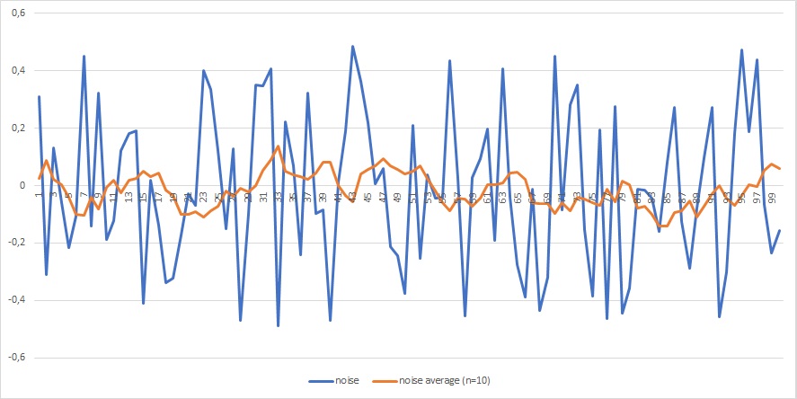
Following picture shows how visible is the benefit in noise reduction averaging a random variable by a factor of 10:
Oversampling
Oversampling consists in sampling the ADC input signal by a frequency that is higher than the required sampling rate fs. In accordance with the Nyquist Theorem, this is usually the Nyquist frequency fn corresponding to, the double of highest frequency component fm of interest in the input signal.
\[
f_s \gt f_n = 2 \cdot f_m
\]
For each additional bit of resolution (see ref. [4] and [5]), the signal must be oversampled by a factor of four, in general the oversampling frequecy fos is given by:
\[
f_{os} = 4^w \cdot f_s
\]
Where w is the number of additional bits of resolution desired.
For example to increase the resolution of the ATmega328P ADC of 2 additional bits (from 10 to 12 bits) we need to oversample by a factor of 16 (42). We need to cumulate 16 consecutive readings and then average the result by 4 (or right shift the sum by 2 bits). This is also referred as decimation process. This way we will have a 12 bit effective sample with an improvement in the SNR (Signal to Noise Ratio).
Circuit design considerations
Following pictures shows the final circuit schema for the current sensor:
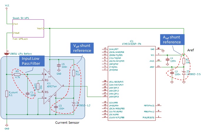
The circuit implements the current sensor design described in previous paragraphs. There are few additional modules required by the circuit whose components need correct sizing:
- Instrumental amplifier input low pass filter
- Voff and Vref voltage shunt regulators
Amplifier input low pass filter
An input low pass filter to the instrumentation amplifier is highly recommended to filter out RF interference. In fact, instrumentation amplifiers can rectify high frequency out of-band signals. Once rectified, these signals appear as dc offset errors at the output. RF interference can be present for example in circuits making use of buck-boost converters that usually operate at frequencies beetween 600Khz and 1.5Mhz. For example the UPS module used in this circuit is using a boost converter to generate a regulated 5V output from the battery voltage.
To suppress these RF interferences, a low pass RC filter can be added to the amplifier input. Resistor R3 and capacitor C1 provide such filter, with a cut off frequency (-3db frequency corresponding to 50% signal power reduction):
\[
f_c = \frac {1}{2 \pi \cdot (R3 \cdot C1)} = \frac {1}{2 \pi \cdot (4,7k\Omega \cdot 100nF)} = 338Hz
\]
R3 and C1 provide a 338Hz cut off frequency that is enough for the purpose of the current sensor, assuming that the measured signal (shunt voltage drop) is quite stable over time.
Voltage shunt regulators
Shunt regulators diodes are used in the circuit to provide a precise and stable voltage reference to the instrumentation amplifier (offset voltage) and the ADC (reference voltage). Diodes used here belong to LM285/385-xxx series from Texas Instruments (see ref. [6]). The LM285/385-xxx are micropower 3-terminal current band-gap voltage reference diodes. They are designed to operate over a wide current range as low as 10µA up to 20mA, with low noise and stable operation over time and temperature. In particular, we selected the LM385z-1.2 for the amplifier offset voltage (Voff) and LN385z-2.5 for the ADC reference voltage (Aref). The regulator circuit is very simple and only requires some precautions in sizing the series resistor to provide the current required by the diode to operate correctly. One important thing to consider is the input impedance of the circuit receiving the refrerence voltage. Following picture shows the typical application circuit:
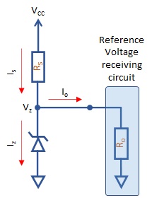
Where:
- Vcc is the unregulated input voltage
- Vz is the shunt regulator (zener) voltage
- Rs is the current limiting resistor
- Ro is the input impedance of the receiving circuit
Iz must be greater than the maximum value of the minimum operating current (Izmin) required by the reference diode. In case of LM385z-xxx the maximum value of the minimum operating current is between 20µA and 30µA over the whole operating temperature range depending on the regulator voltage (see ref. [6]):
\begin{equation} \label{eq:Iz}
I_z = I_s – I_o \gt I_z^{min}
\end{equation}
Where:
\begin{equation} \label{eq:Is}
I_s = \frac{V_{cc} – V_z}{R_s}
\end{equation}
\begin{equation} \label{eq:Io}
I_o = \frac{V_z}{R_o}
\end{equation}
Hence, substituting (\ref{eq:Is}) and (\ref{eq:Io}) in (\ref{eq:Iz}):
\[
I_z = \frac{V_{cc} – V_z}{R_s} – \frac{V_z}{R_o} \gt I_z^{min}
\]
Finally, the constraint on Rs is the following:
\begin{equation} \label{eq:Rs}
R_s \lt \frac {R_o \cdot (V_{cc} – V_z)}{R_o \cdot I_z^{min} + V_z} = \frac {V_{cc} – V_z}{ I_z^{min} + \frac {V_z}{R_o}}
\end{equation}
To reduce power consumption we want to determine the maximum possible value for Rs that results from (\ref{eq:Rs}) replacing the maximum value of the Iz current and the minimum value of Ro resistance. These values can be read from components datasheets.
Amplifier offset shunt regulator
For the shunt regulator connected to the Voff pin of the instrumentation amplifier we have:
Minimum input impedance for AD627 Voff pin (see ref. [2] “AD627 Reference Input Impedance” on Table 3, pag 6) is:
\[
R_o \gt 125k\Omega
\]
Maximum value of the minimum operating current for the shunt diode (see ref. [6] “Minimum Operating Current” max value for LM385-1.2) is:
\[
I_z^{min} \lt 20 \mu A
\]
Substituting above values in (\ref{eq:Rs}):
\[
R_s \lt 126k\Omega
\]
ADC reference shunt regulator
For the shunt regulator connected to the Aref pin of the ATmega328P we have:
Minimum input impedance for ATmega328P Aref pin (see ref. [7] “Reference input resistance” on Table 28-8):
\[
R_o \gt 22.4k\Omega
\]
Maximum value of the minimum operating current for the shunt diode (see ref. [6] “Minimum Operating Current” max value for LM385-2.5) is:
\[
I_z^{min} \lt 30 \mu A
\]
Substituting above values in (\ref{eq:Rs}):
\[
R_s \lt 18k\Omega
\]
References
@article{solarheatingcontroller,
author = "Massimo Morlupi",
title = "{Solar Heating Controller}",
year = "2020"
}[Bibtex]
@ad627{ad627,
author = "Analog Devices",
title = "{Micropower, Single- and Dual-Supply, Rail-to-Rail Instrumentation Amplifier}",
year = "2013"
}@iid{iid,
author = "Howard E. Haber",
title = "{Class Handouts - iid random variables}",
year = "2012"
}@an118{an118,
author = "Silicon Labs",
title = "{Improving ADC Resolution by Oversampling and Averaging}",
year = "rev 1.3"
}@avr121{avr121,
author = "Atmel",
title = "{AVR121: Enhancing ADC resolution by oversampling}",
year = "2005"
}@lmx85{lmx85,
author = "ON Semiconductor",
title = "{LM285/LM385 Micropower Voltage References}",
year = "2016"
}[Bibtex]
@atmega328p{atmega328p,
author = "Atmel Corporation",
title = "{ATmega328P - 8-bit AVR Microcontroller with 32K Bytes In-System Programmable Flash}",
year = "2015"
}

